|
Advanced Material Process
|
New SOI, GOI, SSDOI material using smart cut, wafer bonding, and nano-mechanics are developed for future device applications. New properties of buckled material and nano-strained material are found and will be incorporated to future device design. Related Publications: - W. Hsu, C. -Y. Peng, C. -M. Lin, Y. -Y. Chen, Y. -T. Chen, W. -S. Ho, and C. W. Liu,“Flexible single-crystalline Ge p-channel thin-film transistors with Schottky-barrier source/drain on polyimide substrates,” IEEE Electron Device Letters, Vol. 31, No. 5, pp. 422, 2010.
- W. S. Ho, Y.-H. Dai, Y. Deng, C.-H. Lin, Y.-Y. Chen, C.-H. Lee, and C. W. Liu, “Flexible Ge-on-Polyimide detectors,” Appl. Phys. Lett., Vol. 94, 261107, 2009.
- C.-H. Lin, Y.-T. Chiang, C.-C. Hsu, C.-H. Lee, C.-F. Huang, C.-H. Lai, T.-H. Cheng, and C. W. Liu “Ge-on-glass Detectors,” Appl. Phys. Lett., Vol. 91, 041105, 2007.
|
|
|
CMOS Strain Engineering
|
Beyond 90 nm technology node, the strain engineering is the key technology to boost the channel mobility and enhance the performance of CMOS transistors. Strained engineering process, typically enhancing the CMOS device performance by 10~20 %, benefits from the advantage of low cost, compatibility with CMOS process and high controllability. In addition to the mobility enhancement, strain engineering also helps reduce leakage and improves retention time in non-volatile memory devices.
In the study of CMOS strain engineering, we had great research experiences and strong collaborations with the world-leading electronics companies in Taiwan. Current research projects include 1) strained material growth (ex. Ge/GeSi-on-Si heterostructure), 2) simulation in devices (ex. TSV stress and strain simulation by Ansys) and 3) strain measurement (Raman spectroscopy). 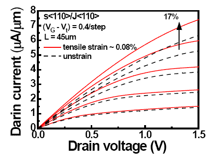 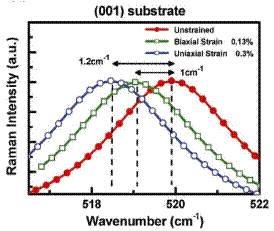
Related Publications: - C.-Y. Peng, Y.-C. Fu, C.-F. Huang, Y.-J. Yang, S.-T. Chang, and C.W. Liu, “Effects of Applied Mechanical Uniaxial and Biaxial Tensile Strain on the Flatband Voltage of (001), (110), and (111) Metal-Oxide-Silicon Capacitors,” IEEE Trans. on Electron Devices, Vol. 56, No. 8, pp. 1736-1745, 2009.
- C.-Y. Peng, C.-F. Huang, Y.-C. Fu, Y.-H. Yang, C.-Y. Lai, S.-T. Chang, and C. W. Liu, “Comprehensive study of the Raman shifts of strained silicon and germanium,” J. Appl. Phys., Vol. 105, 083537, 2009.
- Y.-J. Yang, W. S. Ho, C.-F. Huang, S. T. Chang, and C. W. Liu, “Electron mobility enhancement in strained-germanium n-channel metal-oxide-semiconductor field-effect-transistors,” Appl. Phys. Lett., Vol. 91, 102103, 2007; also in Virtual Journal of Nanoscale Science & Technology, Vol. 16, Issue. 12, 2007.
|
|
|
Si/Ge MOSFET and SiGe HBT Devices
|
The superior transport property of Ge can reach high performance target in the future CMOS technology. The high mobility and compatibility with CMOS process make Ge a promising material in the future high-end device application even though there are still some unresolved issues such as the cost and unstable germanium oxide dielectrics. In this project, we focus on developing the low cost, high performance Ge MOSFETs, which is expected to replace silicon as the future industry mainstream. Many technical solutions such as Ge surface passivation, high K-metal gate (HK-MG) and strain engineering are applied to boost the channel mobility and enhance the device performance and stability. In 2010, we successfully demonstrated the world highest mobility Ge NFETs on (001) Ge substrate (published on IEDM 2010). The record peak mobility of ~1050 cm2/V-s is the highest reported electron mobility on (001) Ge from now. On the other side, the new thermal growth technique of thin film Ge/SiGe on Si wafers is promoted recently. Ge-on-Si material structure can provide Ge MOSFET a cheap and high strained substrate layer. 2010 IEDM Ge nMOSFET device Peak mobility: ~1050 cm2/V-s The SS value: 150mV/dec Device on/off ratio: 2x10⁴. Junction, on/off ratio: 2x10⁵ 2011 IEDM SOI based Ge GAA PFETs Weff/Lg (nm) =260/183 Wfin = 52nm Ion/Ioff ~ 1´105 EOT = 5.5nm S.S = 130 mV/dec 2012 IEDM Triangular Ge NFETs on Si with (111) Sidewalls EOT=0.39 nm ZrO2/Ge Weff/Lg (nm) =186/350 Wfin = 58nm Ion/Ioff ~ 1´104 EOT = 5.5nm S.S = 94 mV/dec Ion: 2 times enhanced Related Publication: - Shu-Han Hsu, Hung-Chih Chang, Chun-Lin Chu, Yen-Ting Chen,Wen-Hsien Tu, Fu Ju Hou, Chih Hung Lo, Po-Jung Sung, Bo-Yuan Chen, Guo-Wei Huang, Guang-Li Luo, C. W. Liu, Chenming Hu, and Fu-Liang Yang, “Triangular-channel Ge NFETs on Si with (111) Sidewall-Enhanced Ion and Nearly Defect-free Channels,” accepted International Electron Devices Meeting (IEDM), 2012.
- Shu-Han Hsu, Chun-Lin Chu, Wen-Hsien Tu, Yen-Chun Fu, Po-Jung Sung, Hung-Chih Chang, Yen-Ting Chen, Li-Yaw Cho, Guang-Li Luo, William Hsu, C. W. Liu, Chenming Hu, and Fu-Liang Yang, Chenming Hu, and Fu-Liang Yang, “ Nearly Defect-free Ge Gate-All-Around FETs on Si Substrates,” International Electron Devices Meeting (IEDM), 2011.
- Yen Chun Fu, William Hsu, Yen-Ting Chen, Huang-Siang Lan, Cheng-Han Lee, Hung-Chih Chang, Hou-Yun Lee, Guang-Li Luo, Chao-Hsin Chien, C. W. Liu, Chenming Hu, and Fu-Liang Yang " High mobility high on/off ratio C-V dispersion-free Ge n-MOSFETs and their strain response," International Electron Devices Meeting (IEDM), 2010.
|
|
|
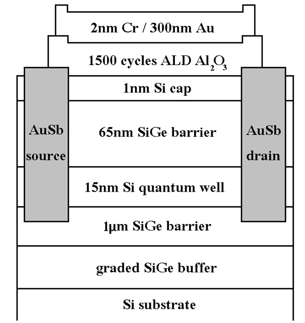
Material growth of SiGe quantum structures
|
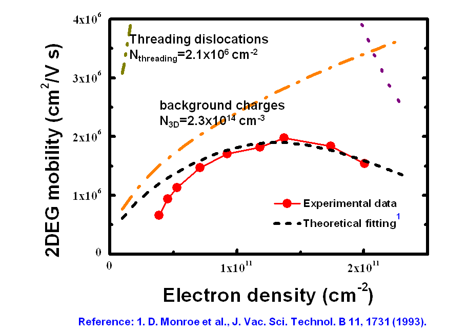
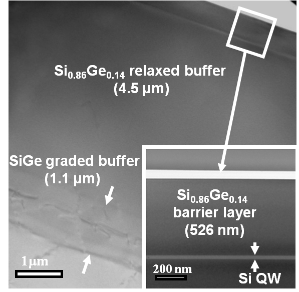
The effect of carrier confinement in quantum structure will arise several interesting physical phenomena such as two-dimensional electronic gases (2DEGs). Among various semiconductor materials, Si-based quantum structures are of particular interest. The ubiquitous characteristics of SiGe quantum structures are in potential application in novel nanoelectronics, photonics and spintronics. In this project, we focus on the material growth of SiGe quantum well. An un-doped SiGe/strained Si/SiGe quantum well was fabricated on p-type Si at 550 ℃ by hot-wall ultrahigh vacuum chemical vapor deposition. In 2012, in collaboration with Nobel Prize laureate, Phof. D. C. Tsui, we reported the undoped 2DEG Si/SiGe QW structure with the extremely high mobility of 2.0x106 cm2/Vs, a record value, at 0.3K for 15 nm Si well with a SiGe barrier layer. The quantum Hall effect characteristics are observed in the enhancement mode insulated-gate field-effect transistors (IGFETs)

Related Publications: - S. -H. Huang, T. -M. Lu, S. -C. Lu, C. -H. Lee, C. W. Liu, and D. C. Tsui, “Mobility enhancement of strained Si by optimized SiGe/Si/SiGe structures,” Appl. Phys. Lett., Vol. 101, 042111, 2012.
- C. -H. Lee, C. W. Liu, H. -T. Chang, and S. W. Lee, "Hexagonal SiGe Quantum Dots and Nanorings on Si(110)," J. Appl. Phys. 107, 056103, 2010APPLIED PHYSICS (SCI, EI) T. M. Lu*, C. -H. Lee, D. C. Tsui, and C. W. Liu, "Integration of complementary circuit and two-dimensional electron gas in a Si/SiGe heterostructure," Appl. Phys. Lett., Vol. 96, 253103, 2010.
- C.-H. Lee, Y.-Y. Shen, C. W. Liu, S. W. Lee, B.-H. Lin, and C.-H. Hsu, "SiGe nanorings by ultrahigh vacuum chemical vapor deposition," Appl. Phys. Lett., Vol. 94, 141909, 2009
- T. M. Lu*, D. C. Tsui, C. -H. Lee and C. W. Liu, "Observation of two-dimensional electron gas in a Si quantum well with mobility of 1.6×106 cm2/Vs," Appl. Phys. Lett., Vol. 94, 182102, 2009.
- C.-H. Lee, C.-Y. Yu, C. M. Lin, C.W. Liu, H. Lin, and W.-H. Chang, "Carrier gas effects on the SiGe quantum dots formation," Applied Surface Science, Vol. 254, No. 19, pp. 6257-6260, 2008.
|
|
|
Research
|
Research areas of Professor Chee Wee Liu (Distinguished/Chair Professor of NTU) 1. SiGe/Ge/GeSn epi technologies for the more Moore and more than Moore applications, including 3D stacked high mobility channel transistors, related gate stack, and Si photonics (Lidar/IR detector/ CMOS image sensor). 2. Mobility/transport calculations, band structure calculation, First principle calculation. 3. Memory technologies : MRAM and DRAM. 4. High mobility IGZO TFT and Si solar cells
Novel Electronics 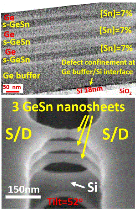 | | Vertically Stacked GeSn Nanosheet pGAAFETs IHigh-quality, fully compressively strained CVD-grown GeSn multi-layers are produced with defects confinement near the Ge buffer/Si interface. With the Ge layers used as sacrificial layers, the optimum ultrasonic-assisted H2O2 etching technique, the low thermal budget gate stack (400 °C), and the S/D parasitic resistance reduction, the first stacked 3-Ge0.93Sn0.07-nanosheets pGAAFET with LCH = 60 nm achieved record high Ion=1975A/m per channel width among all GeSn pFETs. Uniform stacked GeSn nanosheet GAAFETs with low surface roughness are compatible with Si technologies and are good candidates for future technology nodes to extend Moore’s law for CMOS scaling. | | | | | 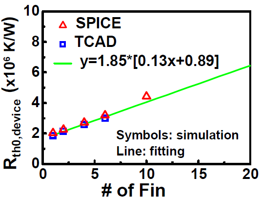 | | Comprehensive thermal modeling of 3D transistors with circuit-level reliablity evaluation Self-heating effect of the 3D transistor is simulated by TCAD. The boundary/alloy scattering, nanostructure effect, and the interfacial thermal resistances (ITRs) are considered. From the results, the device thermal resistances are extracted. In addition, thermal SPICE modeling for the 3D transistor is proposed and verified by the TCAD simulation. Our modularized thermal SPICE model has dependencies on the device geometries, materials, and layouts. It provides frequency-dependent spatial and temporal temperature distribution. Thanks to its less computation cost than the TCAD simulation, the self-heating effect and related reliability issues of small circuits (e.g. 5-stage ring oscillators) are evaluated by our SPICE model. |  | | DRAM TCAD simulation of DRAM capacitor is being developed. The fabrication of DRAM capacitor optimize process condition for DRAM 1x node scaling. Analysis and measurement are used for the reliability issue of DRAM capacitor. | 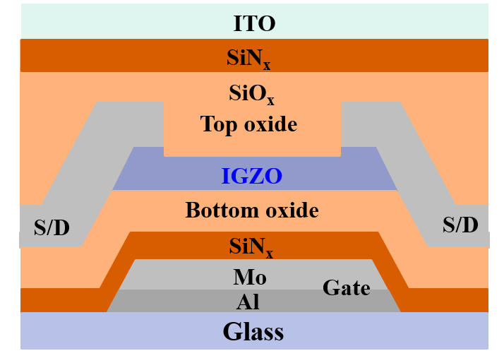 | | IGZO Thin-Film-Transistors (TFTs) The a-IGZO TFTs have higher on/off current ratio (~108) and higher carrier mobility (~28 cm2/ V-s) as compared to amorphous Si (a-Si) TFTs, and is suitable for the high performance applications. | 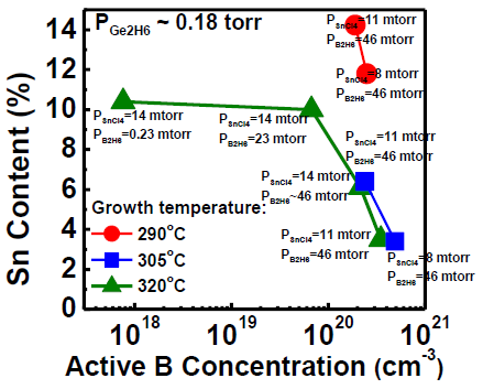 | | In-situ B-doped Epi-GeSn Layers on Ge-buffered Si by CVD In-situ doping by chemical vapor deposition (CVD) has been reported as an efficient method to simultaneously achieve high active dopant concentration and high crystallinity for B-doped GeSn on Ge-buffered Si at low growth temperature of 320oC. To further increase the active dopant concentration and Sn content simultaneously, the epitaxial growth temperature <320oC by CVD is performed. At 320oC, the growth rate of B-doped strained GeSn is 24x enhancement as compared to undoped Ge. By lower the growth temperature to 305oC and 290oC, the active [B] of 4.9x1020 cm-3 and [Sn] of 14.2% are achieved, respectively. The low contact resistivity of 2.4x10⁻⁹ Ω-cm2 for in-situ B-doped epi-GeSn by CVD is demonstrated. | 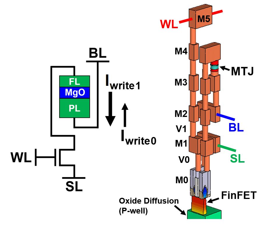 | | MRAM The thermal model of spin-transfer torque MRAM (STT-MRAM) is being developed. The self-heating and the thermal coupling between transistor and magnetic tunnel junction (MTJ) can increase the MTJ temperature. The increasing temperature leads to the degradation of read disturbance and MgO reliability. |  | | Device Modeling and Simulation BSIM and Mextram models are being developed to take the strain and optical effects into account for RF and high speed digital applications. Finite element analyses of ISE-TACD and ANSYS are used to simulate Ge FET and MOS LED/GOI detector theoretically. |
Photonics  |
| Ge/GeSn photonics devices The bandgap tuning and direct bandgap emission of GeSn can enhance the performance of group IV photonic devices on Si platform. |  | | NIR cmos image sensor BSI cmos image sensor with NIR detection can be used in the camera and automobile applications. |  | | Lidar Optical steering can achieve by optical phase array.This technique can be used for the Lidar applications | | | |
Photovoltaic  |
| Quantum efficiency (QE), solar cell efficiency, dark and photo I-V measurement, carrier lifetime measurement by QSSPC, and FTPS for defect level. |
|
|
|
Download
|
出國開會補助 出國開會注意事項 口試注意事項 meal box less than 100 NT(no deep fried food) Water and tea Sandwich if after 5pm Paid by project 各位同學,使用公費購買研究物品及耗材,一定要避免附檔的缺失。有問題隨時與秦小姐和老師討論。 公告毒性化學物質及其管制濃度與大量運作基準一覽表 (本實驗室所有人員禁止使用任何毒化物) Group FTP site: ftp://140.112.21.150:7788 帳號密碼請跟林宗毅申請 Conference & Short Course
2010 IEDM  nanosioe nanosioe
Alternative high-k dielectrics: prospects in silicon, memory and GaN technologies (K. Fröhlich, Institute of Electrical Engineering, SAS, Bratislava, Slovakia) 2011 VLSI Short Course nanosioe
Technical Documents
|
|
|
Journal Paper
|
1996 1997 1998 1999 2000 2001 2002 2003 2004 2005 2006 2007 2008 2009 2010 2011 2012 2013 2014 2015 2016 2017 2018 2018- Hung-Yu Ye, Chia-Che Chung and C. W. Liu, "Mobility Calculation of Ge Nanowire Junctionless and Inversion-Mode Nanowire NFETs With Size and Shape Dependence," in IEEE Transactions on Electron Devices, vol. 65, no. 12, pp. 5295-5300, Dec. 2018
- Chung-Yi Lin, Hung-Yu Ye, Fang-Liang Lu, H. S. Lan, and C. W. Liu, “Biaxial strain effects on photoluminescence of Ge/strained GeSn/Ge quantum well,” Opt. Mater. Express 8, 2795-2802, 2018
- V. T. Dolgopolov, M. Yu. Melnikov, A. A. Shashkin, S.-H. Huang, C. W. Liu, and S. V. Kravchenko, “Fractional Quantum Hall Effect in SiGe/Si/SiGe Quantum Wells in Weak Quantizing Magnetic Fields,” JETP Letters, Vol. 107, No. 12, pp. 794-797, 2018.
- Yu-Shiang Huang, Fang-Liang Lu , Ya-Jui Tsou, Hung-Yu Ye, Shih-Ya Lin, Wen-Hung Huang, and C. W. Liu, ” Vertically Stacked Strained 3-GeSn-Nanosheet pGAAFETs on Si Using GeSn/Ge CVD Epitaxial Growth and the Optimum Selective Channel Release Process”, IEEE Electron Device Letters, Vol. 39, No. 9, pp.1274-1277, 2018.
- Chung-En Tsai, Fang-Liang Lu, Pin-Shiang Chen, and C. W. Liu, “Boron-doping induced Sn loss in GeSn alloys grown by chemical vapor deposition,” Thin Solid Films, Vol. 660, pp. 263-266, 2018.
- Fang-Liang Lu, Chung-En Tsai, I-Hsieh Wong, Chun-Ti Lu, and C. W. Liu, “Dopant Recovery in Epitaxial Ge on SOI by Laser Annealing With Device Applications,” IEEE Transactions on Electron Devices, Vol. 65, No. 7, pp. 2925-2931, 2018.
- E. Bussmann, John King Gamble, J. C. Koepke, D. Laroche, S. H. Huang, Y. Chuang, J.-Y. Li, C. W. Liu, B. S. Swartzentruber, M. P. Lilly, M. S. Carroll, and T.-M. Lu, “Atomic-layer doping of SiGe heterostructures for atomic-precision donor devices,” Physical Review Materials 2, 066004, 2018.
2017- M. Yu. Melnikov, V. T. Dolgopolov, A. A. Shashkin, S.-H. Huang, C. W. Liu, and S. V. Kravchenko, “Unusual anisotropy of inplane field magnetoresistance in ultra-high mobility SiGe/Si/ SiGe quantum wells,” Journal of Applied Physics 122, 224301, 2017.
- M. Yu. Melnikov, A. A. Shashkin, V. T. Dolgopolov, S.-H. Huang, C. W. Liu, and S. V. Kravchenko, “Indication of band flattening at the Fermi level in a strongly correlated electron system,” Scientific Reports 7, 14539, 2017.
- T. M. Lu, C. T. Harris, S.-H. Huang, Y. Chuang, J.-Y. Li, and C. W. Liu, “Effective g factor of low-density two-dimensional holes in a Ge quantum well,” Appl. Phys. Lett., Vol. 111, 102108, 2017.
- Chun-Ti Lu, Fang-Liang Lu, Chung-En Tsai, Wen-Hung Huang, and C. W. Liu, “Process simulation of pulsed laser annealing on epitaxial Ge on Si,” ECS J. Solid State Sci. Tech., Vol. 6, pp. 495-498, 2017.
- T. M. Lu, L. A. Tracy, D. Laroche, S.-H. Huang, Y. Chuang, Y.-H. Su, J.-Y. Li, and C. W. Liu, “Density-controlled quantum Hall ferromagnetic transition in a two-dimensional hole system,” Scientific Reports 7, 2468, 2017.
- Yu-Shiang Huang, Ya-Jui Tsou, Chih-Hsiung Huang, Chih-Hao Huang, Huang-Siang Lan, C. W. Liu, Yi-Chiau Huang, Hua Chung, Chorng-Ping Chang, Schubert S. Chu, and Satheesh Kuppurao.,” High-Mobility CVD-Grown Ge/Strained Ge0.9Sn0.1/Ge Quantum-Well pMOSFETs on Si by Optimizing Ge Cap Thickness”, IEEE Trans. on Electron Devices, Vol. 64, No. 6, pp.2498-2504, 2017.
- H.-S. Lan, S. T. Chang, and C. W. Liu, “Semiconductor, topological semimetal, indirect semimetal, and topological Dirac semimetal phases of Ge1-xSnx alloys,” 95, 201201(R), Phys. Rev. B, Rapid Communication, 2017.
- Chih-Hsiung Huang, Yu-Shiang Huang, Da-Zhi Chang, Tzo-Tao Lin, and C. W. Liu, “Interface trap density reduction due to AlGeO interfacial layer formation by Al capping on Al2O3/GeOx/Ge stack,” IEEE Transactions on Electron Devices, Vol. 64, No. 4, pp. 1412-1417, 2017.
- H.-S. Lan and C. W. Liu, “Band alignments at strained Ge1-xSnx/relaxed Ge1-ySny heterointerfaces,” 50, 13LT02, J. Phys. D: Appl. Phys., 2017.
- Pin-Shiang Chen, Sheng-Ting Fan, Huang-Siang Lan, C. W. Liu, “Band calculation of lonsdaleite Ge,” J. Phys. D: Appl. Phys. 50, 015107, 2017.
2016- Hung-Yu Ye, Huang-Siang Lan, and C. W. Liu, “Electron Mobility in Junctionless Ge Nanowire NFETs,” IEEE Transactions on Electron Devices, Vol. 63, No.11, pp. 4191, 2016.
- Chung-Yi Lin, Chih-Hsiung Huang, Shih-Hsien Huang, Chih-Chiang Chang, C. W. Liu, Yi-Chiau Huan , Hua Chung, Chorng-Ping Chang “Photoluminescence and electroluminescence from Ge⁄strained GeSn⁄Ge quantum wells” Appl. Phys. Lett., Vol. 109, 091103, 2016.
- S.-T. Fan, J.-Y. Yan, D.-C. Lai, C. W. Liu, “The hysteresis-free negative capacitance field effect transistors using non-linear poly capacitance,” Solid-State Electronics, Volume 122, Pages 13-17, 2016.
- X. Zhu, T.-H. Cheng, and C. W. Liu, “Ga Content and Thickness Inhomogeneity Effects on Cu(In, Ga)Se2 Solar Modules”, Electronic Materials Letters, Vol. 12, No. 4, pp. 506-511, 2016.
- D. Laroche, S.-H. Huang, Y. Chuang, J.-Y. Li, C. W. Liu and T. M. Lu, “Magneto-transport analysis of an ultra-low-density two-dimensional hole gas in an undoped strained Ge/SiGe heterostructure,” Appl. Phys. Lett., Vol. 108, 233504, 2016.
- Chun-Ti Lu, Yu-Shiang Huang and C. W. Liu, “Passivation of Al2O3 / TiO2 on monocrystalline Si with relatively low reflectance,” J. Phys. D: Appl. Phys. 49, 245105, 2016.
- Chieh Lo, Zheng-Lun Feng, Wei-Lun Huang, C. W. Liu, T. -L. Chen, and C. H. Chou, “Abnormal Threshold Voltage Shift of Amorphous InGaZnO Thin-film Transistors due to Mobile Sodium,” IEEE J. of Electron Devices Society, Vol. 4, No. 5, pp. 353-357, 2016.
- Shi Luo, Carissa Eisler, Tsun-Hsin Wong, Hai Xiao, Chuan-En Lin, Tsung-Ta Wu, Chang-Hong Shen, Jia-Min Shieh, Chuang-Chuang Tsai, C. W. Liu, Harry A. Atwater, William A. Goddard III, Jiun-Haw Lee, Julia R. Greer, “Suppression of surface recombination in CuInSe2 (CIS) thin films via Trioctylphosphine Sulfide (TOP:S) surface passivation,” Acta Materialia, Volume 106, Pages 171–181, 2016.
T. M. Lu, D. Laroche, S.-H. Huang, Y. Chuang, J.-Y. Li, and C. W. Liu, “High-mobility capacitively-induced two-dimensional electrons in a lateral superlattice potential,” Scientific Reports 6, 20967, 2016. 2015- S.-H. Huang, F.-L. Lu, W.-L. Huang, C.-H. Huang, and C. W. Liu, “The ∼3×1020 cm−3 electron concentration and low specific contact resistivity of phosphorus-doped Ge on Si by in-situ chemical vapor deposition doping and laser annealing”, IEEE Electron Device Letter, Vol. 36, No. 11, pp. 1114-1117, 2015.
- Sun-Rong Jan, Tien-Pei Chou, Che-Yu Yeh, C. W. Liu, Robert V. Goldstein, Valentin A. Gorodtsov, and Pavel S. Shushpannikov “Comments and Corrections Reply to “Comment on ‘A Compact Analytic Model of the Strain Field Induced by Through Silicon Vias”, IEEE Transactions on Electron Devices, Vol. 62, No. 9, pp. 3106, 2015
- Jhih-Yang Yan, Sun-Rong Jan, Yi-Chung Huang, Huang-Siang Lan, Y.-H. Huang, Bigchoug Hung, K.-T. Chan, Michael Huang, M.-T. Yang and C. W. Liu, “Asymmetric Keep-out Zone of Through-Silicon Via using 28nm Technology Node”, IEEE Electron Device Letter, Vol. 36, No. 9, pp. 938-940, 2015.
- I-Hsieh Wong, Yen-Ting Chen, Shih-Hsien Huang, Wen-Hsien Tu, Yu-Sheng Chen and C. W. Liu, “Junctionless Gate-all-around PFETs using in-situ Boron Doped Ge channel on Si”, IEEE Transaction on Nanotechnology, Vol. 14, No. 5, pp. 878-882, 2015.
- Yen-Yu Chen, C.-C. Yen, T.-Y. Chang, C. W. Liu, “Enhance light emission from Ge by GeO2 micro hemispheres”, Solid-State Electronics, Volume 110, Pages 83-85, 2015.
- D. Laroche, S.-H. Huang, E. Nielsen, C. W. Liu, J.-Y. Li, and T. M. Lu, “Magneto-transport of an electron bilayer system in an undoped Si/SiGe double-quantum-well heterostructure,” Appl. Phys. Lett., Vol. 106, 143503, 2015.
- M. Yu. Melnikov, A. A. Shashkin, V. T. Dolgopolov, S.-H. Huang, C. W. Liu, and S. V. Kravchenko,“Ultra-high mobility two-dimensional electron gas in a SiGe/Si/SiGe quantum well,” Appl. Phys. Lett., Vol. 106, 092102, 2015.
2014 - Xiaobo Zhu and C. W. Liu, “Fabrication and characterization of Cu(In,Ga)Se2 p-channel thin film transistors”, Appl. Phys. Lett., Vol. 105, 143502, 2014.
- C.W. Liu, M. Östling, and J.B. Hannon, “New Materials for Post-Si Computing”, MRS Bulletin, Vol. 39, No. 8, pp. 658-662, August, 2014
- Shi Luo, Jiun-Haw Lee, C. W. Liu, Jia-Min Shieh, Chang-Hong Shen, Tsung-Ta Wu ,D. Jang and Julia R. Greer, “Strength, stiffness,and microstructure of Cu(In,Ga)Se2 thin films deposited viasputtering and co-evaporation,” Appl. Phys. Lett. 105, 011907 (2014).
- M. Yu. Melnikov, A. A. Shashkin, V. T. Dolgopolov, S. V. Kravchenko, S.-H. Huang, C. W. Liu, “Effective Electron Mass in High_Mobility SiGe/Si/SiGe Quantum Wells” JETP Letters, Vol. 100, No. 2, pp. 114-119, 2014
- Wen-Hsien Tu, Shu-Han Hsu, and C. W. Liu, “The PN Junctions of Epitaxial Germanium on Silicon by Solid Phase Doping” IEEE Trans. Electron Device, Vol. 61, No. 7, pp. 2595-2598, 2014
- I-Hsieh Wong, Yen-Ting Chen, Jhih-Yang Yan, Huang-Jhih Ciou, Yu-Sheng Chen and C. W. Liu, “Fabrication and Low Temperature Characterization of Ge (110) and (100) p-MOSFETs” IEEE Transactions on Electron Devices, Vol. 61, No. 6, pp. 2215, 2014.
- H. -S. Lan and C. W. Liu, “Ballistic electron transport calculation of strained germanium-tin fin field-effect transistors”, Appl. Phys. Lett., Vol. 104, 192101, 2014.
- Hung-Chih Chang, Cheng-Ming Lin, Chih-Hsiung Huang, and C. W. Liu, “Hysteresis Reduction by Fluorine Incorporation into High Permittivity Tetragonal ZrO2 on Ge”, Appl. Phys. Lett., Vol. 104, 032902, 2014.
2013 - Y. -T. Chen, H. -C. Chang, I. -H. Wong, H. -C. Sun, H. -J. Ciou, W. -T. Yeh, S. -J. Lo, and C. W. Liu, "Radiation Impact of EUV on High Performance Ge MOSFETs," IEEE Electron Device Letters, vol. 34, no. 10, pp. 1220–1222, 2013.
- Ming-Heng Tsai, Sun-Rong Jan, Che-Yu Yeh, C. W. Liu, Robert V. Goldstein, Valentin A. Gorodtsov, and Pavel S. Shushpannikov, "Modeling and Optimization of Edge Dislocation Stressors," IEEE Electron Device Letters, vol. 34, no. 8, pp. 948–950, 2013.
- Cheng-Ming Lin, Hung-Chih Chang, I-Hsieh Wong, Shih-Jan Luo, C. W. Liu, and Chenming Hu, "Interfacial layer reduction and high permittivity tetragonal ZrO2 on germanium reaching ultrathin 0.39 nm equivalent oxide thickness," Appl. Phys. Lett., Vol. 102, 232906, 2013.
- Yen-Yu Chen, H.-C. Chang, Y.-H. Chi, C.-H. Huang, and C. W. Liu, “GeO2 passivation for low surface recombination velocity on Ge surface,” IEEE Electron Device Letters, Vol. 34, No. 3, pp. 444-446, 2013.
- Tsang-Long Chen, Kuan-Chang Huang, Hsuan-Yi. Lin, C. H. Chou, H. H. Lin, and C. W. Liu, “Enhanced Current Drive of Double Gate α-IGZO Thin Film Transistors,” IEEE Electron Device Letters, Vol. 34, No. 3, pp. 417-419, 2013.
- Hsin-Ping Wang , Tzu-Yin Lin , Chia-Wei Hsu ,Meng-Lin Tsai , Chih-Hsiung Huang , Wan-Rou Wei ,Ming-Yi Huang , Yi-Jiunn Chien , Po-Chuan Yang , C. W. Liu , Li-Jen Chou , and Jr-Hau He, “Realizing High-Efficiency Omnidirectional N-Type Si Solar Cells Via The Hierarchical Architecture Concept With Radial Junctions” ACS Nano, 7 (10), pp. 9325–9335, 2013.
- Wan-Rou Wei , Meng-Lin Tsai , Shu-Te Ho , Shih-Hsiang Tai , Cherng-Rong Ho , Shin-Hung Tsai , C. W. Liu, Ren-Jei Chung , and Jr-Hau He, “Above-11%-Efficiency Organic–Inorganic Hybrid Solar Cells with Omnidirectional Harvesting Characteristics by Employing Hierarchical Photon Trapping Structures,” Nano Letters, 13 (8), pp. 3658–3663, 2013.
2012 - T.M. Lu, W. Pan, D.C. Tsui, C.-H. Lee, and C.W. Liu, “The fractional quantum Hall effect of two-dimensional electrons in high-mobility Si/SiGe field-effect transistors,” accepted by Physical Review B, 2012.
- S.-R. Jan, T.-P. Chou, C.-Y. Yeh, C. W. Liu, R. V. Goldstein, V. A. Gorodtsov, and P. S. Shushpannikov, “A Compact Analytic Model of the Strain Field Induced by Through Silicon Vias,” to be published on IEEE Transactions on Electron Devices, 2012.
- W.-W. Hsu, J. Y. Chen, T.-H. Cheng, S. C. Lu, W.-S. Ho, Y.-Y. Chen, Y.-J. Chien, and C. W. Liu, “Surface passivation of Cu(In,Ga)Se2 using atomic layer deposited Al2O3,” Appl. Phys. Lett., Vol. 100, 023508, 2012.
- C.W. Liu, T.-H. Cheng, Y.-Y. Chen, S.-R. Jan, C.-Y. Chen , S.T. Chan, Y.-H. Nien, Y. Yamamoto, and B. Tillack, “Direct and indirect radiative recombination from Ge,” Thin Solid Films, Vol. 520, pp. 3249–3254, 2012.
2011 - K.-M. Chen, G.-W. Huang, B.-Y. Chen, C.-S. Chiu, C.-H. Hsiao, W.-S. Liao, M.-Y. Chen, Y.-C. Yang, K.-L. Wang, and C. W. Liu, “LDMOS Transistor High-Frequency Performance Enhancements by Strain,” accepted by IEEE Electron Device Letters, 2011.
- T.M. Lu, C.-H. Lee, S.-H. Huang, D.C. Tsui, and C.W. Liu, "Upper limit of two-dimensional electron density in enhancement-mode Si/SiGe heterostructure field-effect transistors," Appl. Phys. Lett., Vol. 99, 153510, 2011.
- H. -S. Lan, Y.-T. Chen, Hung-Chih Chang, J.-Y. Lin, William Hsu, W. -C. Chang, and C. W. Liu, "Electron scattering in Ge metal-oxide-semiconductor field-effect transistors," Appl. Phys. Lett., Vol. 99, 112109, 2011.
- W. S. Ho, Y. Deng, Y.-Y. Chen, T.-H. Cheng, C. W. Liu, W.-F. Tsai, and C.-F. Ai, “Enhanced optical performance by energetic hydrogen passivation at Si/oxide interface,” Thin Solid Films, Vol. 520, pp. 448-451, 2011.
- Y.-Y. Chen, J. Y. Chen, R.-J. Hsu, W. S. Ho, C. W. Liu, W.-F. Tsai, and C.-F. Ai, “Edge passivation of Si solar cells by omnidirectional hydrogen plasma implantation” Journal of The Electrochemical Society, Vol. 158, No. 9, pp. H912-H914, 2011.
- Y.-T. Chen, H.-S. Lan, W. Hsu, Y.-C. Fu, J.-Y. Lin, and C. W. Liu, "Strain response of high mobility germanium n-channel metal-oxide-semiconductor field-effect transistors on (001) substrates," Appl. Phys. Lett., Vol. 99, 022106, 2011.
- S.-H. Tang, E. Y. Chang, M. Hudait, J.-S. Maa, C. W. Liu, G.-L.Luo, H.-D. Trinh, and Y.-H. Su, "High quality Ge thin film grown by ultrahigh vacuum chemical vapor deposition on GaAs substrate," Appl. Phys. Lett., Vol. 98, 161905, 2011.
- Y.-T. Chen , H. -S. Lan , William Hsu , Y.-C. Fu and C. W. Liu , “Strain response of high mobility Germanium n-channel metal-oxide-semiconductor field-effect transistors on (001) substrates” accepted by Appl. Phys. Lett., 2011.
- S. -R. Jan, C. -Y. Chen, C. -H. Lee, S. -T. Chan, K. -L. Peng and C. W. Liu, “Influence of defects and interface on radiative transition of Ge” accepted by Appl. Phys. Lett., 2011.
- H. -S. Lan, S. -T. Chan, T. -H. Cheng, C. -Y. Chen, S. -R. Jan and C. W. Liu, “Biaxial tensile strain effects on photoluminescence of different orientated Ge wafers” accepted by Appl. Phys. Lett., 2011.
- Cheng-Ming Lin, Yen-Ting Chen, Cheng-Hang Lee, Hung-Chih Chang, Wei-Chiang Chang, Huan-Lin Chang, and C. W. Liu, “Voltage Linearity Improvement of HfO2-Based Metal-Insulator-Metal Capacitors with H2O Prepulse Treatment” Journal of The Electrochemical Society, Vol. 158, No. 2, H128, 2011.
2010 - (SCI, EI) H.-C. Sun, C.-F. Huang, Y.-T. Chen, T.-Y. Wu, C. W. Liu, Y.-J. Hsu, and J.-S. Chen “Threshold Voltage and Mobility Extraction of NBTI Degradation of Poly-Si Thin-Film Transistors” IEEE Transactions on Electron Devices,Vol. 57, No. 11, pp. 3186, 2010.
- (SCI, EI) Wen-Wei Hsu, Chao-Yun Lai, C. W. Liu, Chih-Hsin Ko, Ta-Ming Kuan, Tzu-Juei Wang, Wen-Chin Lee, and Clement H. Wann “Insulating Halos to Boost Planar NMOSFET Performance” IEEE Transactions on Electron Devices,Vol. 57, No. 10, pp. 2526, 2010.
- (SCI, EI) Yen-Ting Chen, Hung-Chang Sun, Ching-Fang Huang, Ting-Yun Wu, C. W. Liu, Yuan-Jun Hsu, and Jim-Shone Chen “Capacitorless 1T Memory Cells Using Channel Traps at grain boundaries,” IEEE Electron Device Letters, Vol. 31, No. 10, pp. 1125, 2010.
- (SCI, EI) W. Hsu, C. -Y. Peng, C. -M. Lin, Y. -Y. Chen, Y. -T. Chen, W. -S. Ho, and C. W. Liu,“Flexible single-crystalline Ge p-channel thin-film transistors with Schottky-barrier source/drain on polyimide substrates,” IEEE Electron Device Letters, Vol. 31, No. 5, pp. 422, 2010.
- (SCI, EI) T. -H. Cheng, K. -L. Peng, C. -Y. Ko, C. -Y. Chen, H. -S. Lan, Y. -R. Wu, C. W. Liu, and H. -H. Tseng, “Strain-enhanced photoluminescence from Ge direct transition,” Appl. Phys. Lett., Vol. 96, 211108, 2010.
- (SCI, EI) T. M. Lu*, C. -H. Lee, D. C. Tsui, and C. W. Liu, “Integration of complementary circuit and two-dimensional electron gas in a Si/SiGe heterostructure,” Appl. Phys. Lett., Vol. 96, 253103, 2010.
- (SCI, EI) C. -H. Lee, C. W. Liu, H. -T. Chang, and S. W. Lee, “Hexagonal SiGe Quantum Dots and Nanorings on Si(110),” J. Appl. Phys. 107, 056103, 2010
- (SCI, EI) T. -H. Cheng, C. -Y. Ko, C. -Y. Chen, K. -L. Peng, G. -L. Luo, C. W. Liu, and H. -H. Tseng, “Competitiveness between direct and indirect radiative transitions of Ge,” Appl. Phys. Lett., Vol. 96, 091105, 2010.
- (SCI, EI) S. W. Lee, H. T. Chang,C. -H. Lee, S. L. Cheng and C. W. Liu, “Composition redistribution of self-assembled Ge islands on Si (001) during annealing,” Thin Solid Film, Vol. 518, pp. S196, 2010.
- (SCI, EI) C.-H. Lin* and C. W. Liu, “Metal-oxide-semiconductor SiGe/Si quantum dot infrared photodetectors with delta doping in different positions,” Thin Solid Films, Vol. 518, pp. S237-S240, 2010.
2009 - (SCI, EI) S. W. Lee, C. -H. Lee, H. T. Chang, S. L. Cheng and C. W. Liu, “Evolution of composition distribution of Si-capped Ge islands on Si(001),” Thin Solid Film, Vol. 517, pp. 5029, 2009
- W. -L. Hsu, Y. -H. Pai, F. -S. Meng, C. W. Liu, and G. -R. Lin, “Nanograin crystalline transformation enhanced UV transparency of annealing refined indium tin oxide film,” Appl. Phys. Lett., Vol. 93(23), 231906 - 231906-3, 2009.
- (SCI, EI) C.-Y. Peng, Y.-C. Fu, C.-F. Huang, Y.-J. Yang, S.-T. Chang, and C.W. Liu, “Effects of Applied Mechanical Uniaxial and Biaxial Tensile Strain on the Flatband Voltage of (001), (110), and (111) Metal-Oxide-Silicon Capacitors,” IEEE Trans. on Electron Devices, Vol. 56, No. 8, pp. 1736-1745, 2009.
- (SCI, EI) W. S. Ho, Y.-H. Dai, Y. Deng, C.-H. Lin, Y.-Y. Chen, C.-H. Lee, and C. W. Liu, “Flexible Ge-on-Polyimide detectors,” Appl. Phys. Lett., Vol. 94, 261107, 2009.
- (SCI, EI) T. M. Lu*, D. C. Tsui, C. -H. Lee and C. W. Liu, “Observation of two-dimensional electron gas in a Si quantum well with mobility of 1.6×106 cm2/Vs,” Appl. Phys. Lett., Vol. 94, 182102, 2009.
- (SCI, EI) C.-Y. Peng, C.-F. Huang, Y.-C. Fu, Y.-H. Yang, C.-Y. Lai, S.-T. Chang, and C. W. Liu, “Comprehensive study of the Raman shifts of strained silicon and germanium,” J. Appl. Phys., Vol. 105, 083537, 2009.
- (SCI, EI) P.-S. Kuo, C.-Y. Peng, C.-H. Lee, Y.-Y. Shen, H.-C. Chang, and C. W. Liu, “Si/Si0.2Ge0.8/Si quantum well Schottky barrier diodes,” Appl. Phys. Lett., Vol. 94, 103512, 2009.
- (SCI, EI) T.-H. Cheng, P.-S. Kuo, C.-Y. Ko, and C.-Y. Chen, and C. W. Liu, “Electroluminescence from monocrystalline silicon solar cell,” J. Appl. Phys., Vol. 105, 106107,2009.
- (SCI, EI) C.-H. Lin, Y.-J. Yang, E. Encinas, W.-Y. Chen, J.-J. Tsai, and C. W. Liu, “Single crystalline film on glass for thin film solar cells,” J. Nanosci. Nanotech., Vol. 9, No. 6, pp. 3622-3626, 2009.
- (SCI, EI) C.-H. Lee, Y.-Y. Shen, C. W. Liu, S. W. Lee, B.-H. Lin, and C.-H. Hsu, “SiGe nanorings by ultrahigh vacuum chemical vapor deposition,” Appl. Phys
|
|
|
Conference Paper
|
1995 1996 1997 1998 1999 2000 2001 2002 2003 2004 2005 2006 2007 2008 2009 2010 2011 2012 2013 2014 2015 2016 2017 2018 2018- M. H. Lee, K.-T. Chen, C.-Y. Liao, S.-S. Gu, G.-Y. Siang, Y.-C. Chou, H.-Y. Chen, J. Le, R.-C. Hong, Z.-Y. Wang, S.-Y. Chen, P.-G. Chen, M. Tang, Y.-D. Lin, H.-Y. Lee, K.-S. Li, and C. W. Liu, “Extremely Steep Switch of Negative-Capacitance Nanosheet GAA-FETs and FinFETs,” IEEE International Electron Devices Meeting (IEDM), San Francisco, California, Dec. 1-5, 2018.
- Zong-You Luo, Ya-Jui Tsou, and C. W. Liu, “Field-Free Spin-Orbit Torque Switching of pMTJ Utilizing Voltage-Controlled Magnetic Anisotropy and STT,” IEDM MRAM workshop, San Francisco, California, Dec. 1-6, 2018.
- Ya-Jui Tsou, Zong-You Luo, Chia-Che Chung, and C. W. Liu, “Thermal Modeling of FinFET-Driven Spin-Orbit Torque MRAM Considering Thermal Coupling and BEOL Effects,” IEDM MRAM workshop, San Francisco, California, Dec. 1-6, 2018.
- Hung-Yu Ye, Chia-Che Chung, and C. W. Liu, “Electron Mobility Enhancement by Tensile Strain in Germanium Nanowire NFETs considering surface roughness, channel dopant charge, interface charge, and phonon scattering,” 49th IEEE Semiconductor Interface Specialists Conference(SISC), San Diego, CA, Dec. 5-8, 2018.
- Fang-Liang Lu, Chung-En Tsai, Shih-Ya Lin, and C. W. Liu, “In-situ B-doped Epi-GeSn Layers on Ge-buffered Si by Chemical Vapor Deposition with High Activation (4.9x1020cm-3), High Sn Content (14%), and High Growth Rate Enhancement (24x),” 49th IEEE Semiconductor Interface Specialists Conference, San Diego, CA, Dec. 5-8, 2018.
- (invited) C. W. Liu, Yu-Shiang Huang, Fang-Liang Lu, and Hung-Yu Ye “Ge/GeSn processes and transistor applications,” Americas International Meeting on Electrochemistry and Solid State Science (AiMES), Cancun, Mexico, Sep. 30-Oct. 4, 2018.
- Jhih-Yang Yan, Chia-Che Chung, Sun-Rong Jan, H. H. Lin, W. K. Wan, M.-T. Yang, and C. W. Liu, "Comprehensive Thermal SPICE Modeling of FinFETs and BEOL with Layout Flexibility Considering Frequency Dependent Thermal Time Constant, 3D Heat Flows, Boundary/Alloy Scattering, and Interfacial Thermal Resistance with Circuit Level Reliability Evaluation," Symposium on VLSI Technology (VLSI-Technology), Honolulu , Hawaii, June 18-22, 2018.
- Chih-Hsiung Huang, Da-Zhi Chang, and C. W. Liu, "Annealing Effects on Al2O3/GeOx/Ge Stack with Al and Pt Electrodes," 1st Joint ISTDM / ICSI 2018 Conference, Potsdam (Berlin), Germany, May 27-31, 2018.
- Chung-En Tsai, Fang-Liang Lu, Pin-Shiang Chen, and C. W. Liu, “Dopant Effects in Epitaxial GeSn Layers on Si by CVD,” 1st Joint ISTDM / ICSI 2018 Conference, Potsdam (Berlin), Germany, May 27-31, 2018.
- Hung-Yu Ye, Chia-Che Chung, I-Hsieh Wong, Huang-Siang Lan, C. W. Liu, "Mobility calculation of Ge nanowire junctionless NFETs with size and geometry dependence," 2018 International Symposium on VLSI Technology, Systems and Application (VLSI-TSA), Hsinchu, 2018, pp. 1-2.
- Pin-Shiang Chen, Shou-Chung Lee, A. S. Oates, and C. W. Liu, “BEOL TDDB Reliability Modeling and Lifetime Prediction Using Critical Energy to Breakdown,” IEEE International Reliability Physics Symposium, Burlingame, CA, March 11-15, 2018.
- Matthew Freeman, Tzu-Ming Lu, Yen Chuang, Jiun-Yun Li, C. W. Liu, Jeremy Curtis, and Lloyd Engel, “Microwave Spectroscopy of Resistive Film Gated Higfets and Mosfets,” APS March Meeting, Los Angeles, CA, Mar. 5-9, 2018.
2017 - Yu-Shiang Huang, Fang-Liang Lu, Ya-Jui Tsou, Chung-En Tsai, Chung-Yi Lin, Chih-Hao Huang, and C. W. Liu, “First Vertically Stacked GeSn Nanowire pGAAFETs with Ion=1850mA/mm (VOV=VDS=-1V) on Si by GeSn/Ge CVD Epitaxial Growth and Optimum Selective Etching,” p.832-835, International Electron Devices Meeting (IEDM), 2017.
- M. H. Lee, P.-G. Chen, S.-T. Fan, Y.-C. Chou, C.-Y. Kuo, C.-H. Tang, H.-H. Chen, S.-S. Gu, R.-C. Hong, Z.-Y. Wang, S.-Y. Chen, C.-Y. Liao, K.-T. Chen, S. T. Chang, M.-H. Liao, K.-S. Li, and C. W. Liu, “Ferroelectric Al:HfO2 Negative Capacitance FETs,” p.565-568, International Electron Devices Meeting (IEDM), 2017.
- Fang-Liang Lu, Chung-En Tsai, Pin-Shiang Chen, and C. W. Liu, “Doping Effects on Sn Loss in Epi-GeSn on Si by CVD,” 48th IEEE Semiconductor Interface Specialists Conference, San Diego, CA, Dec. 6-9, 2017.
- Chung-Yi Lin, H.-S Lan, and C. W. Liu, “Photoluminescence and electroluminescence of strained GeSn quantum wells,” 48th IEEE Semiconductor Interface Specialists Conference, San Diego, CA, Dec. 6-9, 2017.
- (invited) C. W. Liu, I-Hsieh Wong, Fang-Liang Lu and Yu-Shiang Huang, "Epitaxial Ge/GeSn high mobility channel transistors," 232nd Meeting of Electrochemical Society, National Harbor, MD, Oct. 1-6, 2017.
- Fang-Liang Lu, Chung-En Tsai, Shih-Ya Lin, Chih-Chiang Chang, and C. W. Liu, “In-situ P-doped and B-doped epi-GeSn on thin Ge buffer layers on Si with low contact resistivity of 1.1x10⁻⁶ (GeSn:P) and 1.9x10⁻⁸ (GeSn:B) Ω-cm2,” 10th International Conference on Silicon Epitaxy and Heterostructures (ICSI-10), Coventry, UK, May 14-19, 2017.
- (invited) C. W. Liu, Fang-Liang Lu, Yu-Shiang Huang, I-Hsieh Wong, “High Performance Ge and GeSn Epi Channels," materials research society (MRS) spring meeting & exhibit, Phoenix, Arizona, Apr. 17-21, 2017.
2016 - Fang-Liang Lu, I-Hsieh Wong, Shih-Hsien Huang, and C. W. Liu, “Tensile strain recovery and dopant re-activation using laser annealing,” 47th IEEE Semiconductor Interface Specialists Conference, San Diego, CA, Dec. 7-10, 2016.
- Chung-Yi Lin, Fang-Liang Lu, C. W. Liu, Yi-Chiau Huang, Hua Chung, and Chorng-Ping Chang, “Passivation and photo/electro luminescence of Ge/GeSn/Ge quantum wells,” 47th IEEE Semiconductor Interface Specialists Conference, San Diego, CA, Dec. 7-10, 2016.
- Jhih-Yang Yan, Sun-Rong Jan, Yu-Jiun Peng, H. H. Lin, W. K. Wan, Y.-H. Huang, Bigchoug Hung, K.-T. Chan, Michael Huang, M.-T. Yang, and C. W. Liu, “Thermal Resistance Modeling of Back-end Interconnect and Intrinsic FinFETs, and Transient Simulation of Inverters with Capacitive Loading Effects,” p.898-901, International Electron Devices Meeting (IEDM), 2016.
- Yu-Shiang Huang, Chih-Hsiung Huang, Fang-Liang Lu, Chung-Yi Lin, Hung-Yu Ye,I-Hsieh Wong, Sun-Rong Jan, Huang-Siang Lan, C. W. Liu, Yi-Chiau Huang, Hua Chung, Chorng-Ping Chang, Schubert S. Chu, and Satheesh Kuppurao “Record High Mobility (428cm2/V-s) of CVD-grown Ge/Strained Ge0.91Sn0.09 /Ge Quantum Well p-MOSFETs,” p.822-825, International Electron Devices Meeting (IEDM), 2016.
- I-Hsieh Wong, Fang-Liang Lu, Shih-Hsien Huang, Hung-Yu Ye, Chun-Ti Lu, Jhih-Yang Yan, Yu-Cheng Shen, Yu-Jiun Peng, Huang-Siang Lan, and C. W. Liu, “High Performance Ge Junctionless Gate-all-around NFETs with Simultaneous Ion =1235 mA/mm at VOV=VDS=1V, SS=95 mV/dec, high Ion/Ioff=2E6, and Reduced Noise Power Density using S/D Dopant Recovery by Selective Laser Annealing,” p.842-845, International Electron Devices Meeting (IEDM), 2016.
- M. H. Lee, S.-T. Fan , C.-H. Tang , P.-G. Chen, Y.-C. Chou , H.-H. Chen , J.-Y. Kuo , M.-J. Xie, S.-N. Liu , M.-H. Liao , C.-A. Jong , K.-S. Li , M.-C. Chen , and C. W. Liu, "Physical Thickness 1.x nm Ferroelectric HfZrOx Negative Capacitance FETs,” p.306-309, International Electron Devices Meeting (IEDM), 2016.
- (invited) C. W. Liu, Jhih-Yang Yan, and Sun-Rong Jan, “Modeling and Simulation of TSV Induced Keep-out Zone Using Silicon Data,” 13th International Conference on Solid-State Integrated Circuit & Technology (ICSICT 2016), Hangzhou, China, Oct. 25-28, 2016.
- Chih-Hsiung Huang, Sheng-Ting Fan, Pin-Shiang Chen, Raman Sankar, F. C. Chou and C. W. Liu, “Atomically Flat Metal-Insulator-Metal Capacitors with Enhanced Linearity,” 22th IEEE Silicon Nanoelectronics Workshop (SNW), Honolulu, USA, June 12-13, 2016.
- Yu-Shiang Huang, Chih-Hao Huang, Chih-Hsiung Huang, Fang-Liang Lu, Da-Zhi Chang, Chung-Yi Lin, I-Hsieh Wong, Sun-Rong Jan, Huang-Siang Lan, C. W. Liu, Yi-Chiau Huang, Hua Chung, Chorng-Ping Chang, Schubert S. Chu, and Satheesh Kuppurao, “Strained Ge0.91Sn0.09 Quantum Well p-MOSFETs,” 22th IEEE Silicon Nanoelectronics Workshop (SNW), Honolulu, USA, June 12-13, 2016.
- S.-H. Huang, F.-L. Lu, S. V. Kravchenko, and C. W. Liu, “Record High Electron Mobility of 2.4 × 106 cm2/V s in Strained Si by Ultra-low Background Doping,” 8th International SiGe Technology and Device Meeting (ISTDM), Nagoya, Japan, June 7-11, 2016.
- F. -L. Lu, S. -H. Huang, and C. W. Liu, "Heavily Phosphorus-doped Si0.1Ge0.9 and Ge on Si with Low Contact Resistivity by Chemical Vapor Deposition and Laser Annealing," 8th International SiGe Technology and Device Meeting (ISTDM), Nagoya, Japan, June 7-11, 2016.
- S. -H. Huang, F. -L. Lu, and C. W. Liu, “Low Contact Resistivity (1.5×10⁻⁸ Ω-cm2) of Phosphorus-doped Ge by In-situ Chemical Vapor Deposition Doping and Laser Annealing,” International Symposium on VLSI Technology, Systems and Applications (VLSI-TSA), Hsinchu, Taiwan, 2016.
- Jhih-Yang Yan, Sun-Rong Jan, Yi-Chung Huang, Huang-Siang Lan, C. W. Liu, Y.-H. Huang, Bigchoug Hung, K.-T. Chan, Michael Huang, and M.-T. Yang, “Compact Modeling and Simulation of TSV with Experimental Verification,” International Symposium on VLSI Technology, Systems and Applications (VLSI-TSA), Hsinchu, Taiwan, 2016.
- T. M. Lu, D. Laroche, S.-H. Huang, E. Nielsen, Y. Chuang, J.-Y. Li, and C. W. Liu, “Electron bilayers in an undoped Si/SiGe double-quantum-well heterostructure,” APS March Meeting, Baltimore, Maryland, Mar. 14-18, 2016.
- D. Laroche, S.-H. Huang, E. Nielsen, Y. Chuang, J.-Y. Li, C. W. Liu, and T. M. Lu, “Scattering mechanisms in shallow undoped Si/SiGe quantum wells,” APS March Meeting, Baltimore, Maryland, Mar. 14-18, 2016.
2015 - Chung-Yi Lin, Shih-Hsien Huang, Chun-Ti Lu, C. W. Liu, ,Yi-Chiau Huang, Hua Chung, and Chorng-Ping Chang “Surface Passivation of Ge/GeSn/Ge Using Atomic Layer Deposited SiO2 and Al2O3,” 46th IEEE Semiconductor Interface Specialists Conference, Arlington, Virginia, Dec. 2-5, 2015.
- Yu-Shiang Huang, Chih-Hsiung Huang, Chung-Yi Lin and C. W. Liu, “Enhanced performance of Y-GeO2/Ge Gate Dielectric by O2 Post-deposition Annealing and Al Capping,” 46th IEEE Semiconductor Interface Specialists Conference, Arlington, Virginia, Dec. 2-5, 2015.
- Chun-Ti Lu, Wenchao Wu and C. W. Liu, “3D Simulation and Analysis of Crystalline Silicon Solar Cell-to-Module Optical Gain,” 25th International Photovoltaic Science and Engineering Conference (PVSEC-25), Busan, Korea, Nov. 15-20, 2015.
- Xiaobo Zhu and C. W. Liu, “Effects of fluctuation on Cu(In,Ga)Se2 solar modules using 3D simulation,” 25th International Photovoltaic Science and Engineering Conference (PVSEC-25), Busan, Korea, Nov. 15-20, 2015.
- (invited) C. W. Liu, Shih-Hsien Huang, and I-Hsieh Wong, “High mobility Si and Ge” SemiconNano, Hsinchu, Taiwan, Sep. 7, 2015.
- (invited) C. W. Liu, I-Hsieh Wong, Yen-Ting Chen and Shu-Han Hsu, “High Mobility Ge Channel Transistors,” Advanced Materials World Congress, Stockholm, Sweden, Aug. 23-26, 2015.
- (invited) C. W. Liu, I-Hsieh Wong, Shih-Hsien Huang and Chih-Hsiung Huang, “3D Ge nanowire transistors,” IEEE Nanotechnology Materials and Devices Conference (NMDC), Anchorage, Alaska, Sep. 13-16, 2015.
- (invited) C.W. Liu, I.-H. Wong, S.-H. Huang, C.-H. Huang and S.-H. Hsu, “Advanced Germanium Channel Transistors,” 11th International Conference on ASIC (ASICON 2015), Chengdu, China, Nov. 3-6, 2015.
- Shi Luo, Eason Lin, Hai Xiao, Jiun-Haw Lee, C. W. Liu, William Goddard, and Julia R. Greer, “Effects of Trioctylphosphine Sulfide Passivation on Na Transport within CuInSe2Thin Films,” MRS spring meeting, San Francisco, Symposium B, paper. No. 9.10. 2015.
- I-Hsieh Wong, Yen-Ting Chen, Shih-Hsien Huang, Wen-Hsien Tu, Chih-Hsiung Huang, Yu-Sheng Chen, Tai-Cheng Shieh and C. W. Liu, “Junctionless Gate-all-around pFETs on Si with In-situ Doped Ge Channel” International Symposium on VLSI Technology, Systems and Applications (VLSI-TSA), Hsinchu, Taiwan, 2015.
2014 - Chun-Ti Lu, Qing-Qi Chen, and C. W. Liu, “Al2O3/TiO2 bilayers as passivation and antireflection coating on silicon,” 45th Semiconductor Interface Specialists Conference, 2014.
- I-Hsieh Wong, Yen-Ting Chen, Shih-Hsien Huang, Wen-Hsien Tu, Yu-Sheng Chen, Tai-Cheng Shieh, Tzu-Yao Lin, Huang-Siang Lan, and C. W. Liu, “In-situ Doped and Tensily Stained Ge Junctionless Gate-all-around nFETs on SOI Featuring Ion = 828 uA/um, Ion/Ioff ~ 1E5, DIBL= 16-54 mV/V, and 1.4X External Strain Enhancement” p.239-242, International Electron Devices Meeting (IEDM), 2014.
- (invited) C. W. Liu, Y.-T Chen, and S.-H Hsu "Gate-all-around Ge FETs" 226th Meeting of Electrochemical Society, Cancun, Mexico, Oct. 5-10, 2014.
- (invited) C. W. Liu, I-Hsieh Wong, Yen-Ting Chen, Wen-Hsien Tu, Shih-Hsien Huang, and Shu-Han Hsu, “Ge Gate-All-Around FETs on Si,” IEEE 12th International Conference on Solid-State and Integrated Circuit Technology (IEEE-ICSICT), Guilin, China, Oct. 2014.
- (invited) C. W. Liu, Yen-Yu Chen, and Wen-Hsien Tu, "SiGe/Ge epi films with photonic and electrical applications." Science & Applications of Thin Films, Conference & Exhibition (SATF 2014), Turkey, September 15-19, 2014.
- (invited) C. W. Liu, "High Mobility Ge Channel Transistors" ISMEN (International Symposium on Materials for Enabling Nanodevices), Tainan, Taiwan, Sep 5, 2014
- Yen-Yu Chen, Chia-Chun Yen, Yi-Hsin Nien, Wen-Wei Hsu, Qing-Qi Chen, and C. W. Liu, “Reabsorption effects on direct band gap emission from germanium light emitting diodes,” The 11th International Conference on Group IV Photonics, Paris, Aug. 27-29, 2014.
- Yen-Yu Chen, T.-Y. Chang, C.-C. Yen, and C. W. Liu, “Enhanced light extraction of Ge by GeO2 micro hemispheres,” 7th International SiGe Technology and Device Meeting (ISTDM), Singapore, June 2-4, 2014.
- H.-S. Lan, and C. W. Liu, “Electron Ballistic Current Enhancement of Ge1-xSnx FinFETs” International Symposium on VLSI Technology, Systems and Applications (VLSI-TSA), Hsinchu, Taiwan, 2014.
- Hung-Chih Chang, Pin-Shiang Chen, Fu-Liang Yang, and C. W. Liu, “Strain Response of Monolayer MoS2 in The Ballistic Regime” International Symposium on VLSI Technology, Systems and Applications (VLSI-TSA), Hsinchu, Taiwan, 2014.
2013 - Jhih-Yang Yan, Pin-Shiang Chen, Jiun-Ian Pai, Wen-Wei Hsu and C. W. Liu, “The Incorporation of Electromagnetic Effects on Through Silicon Vias in TCAD Simulation” International Semiconductor Device Research Symposium, 2013.
- Pin-Shiang Chen, Hung-Chih Chang, Jhih-Yang Yan and C. W. Liu, “Strain Response of Monolayer MoS2 under Ballistic Limit” International Semiconductor Device Research Symposium, 2013.
- I-Hsieh Wong, Yen-Ting Chen, Shih-Hsien Huang, Wen-Hsien Tu, Chih-Hsiung Huang, Yu-Sheng Chen, Chun-Liu Chu, Shu-Han Hsu and C. W. Liu, “High Performance Junctionless In-situ Doped Ge Gate-all-around PFETs on Si” International Semiconductor Device Research Symposium, 2013.
- Chih-Hsiung Huang, Cheng-Ming Lin, Hung-Chih Chang and C. W. Liu, “Post-Gate Fluorine Incorporation by CF4 Plasma on Very High Tetragonal ZrO2/Ge Gate Stack with Ultrathin EOT of 0.4 nm,” 44th Semiconductor Interface Specialists Conference, 2013.
- Ya-Shiun Wu ,Yen-Yu Chen , C.-H. Huang, and C. W. Liu, “High efficient N-type solar cells using ion implanted emitters and back surface field,” 23rd International Photovoltaic Science and Engineering Conference (PVSEC-23), 2013.
- (invited) C. W. Liu, Hung-Chih Chang, Yen-Ting Chen, Wen-Hsien Tu, I-Hsieh Wong, Shu-Han Hsu, and Chun-Lin Chu, “3D Ge transistors,” IEEE Nanotechnology Materials and Devices Conference (IEEE-NMDC), Tainan, Taiwan, Oct. 2013.
- Hung-Chih Chang, Pin-Shiang Chen, and C. W. Liu “Tensile Strain Responses and Dielectric Effect on Monolayer MoS2,” IEEE Nanotechnology Materials and Devices Conference (IEEE-NMDC), Tainan, Taiwan, Oct. 2013.
- Jheng-Sin Liu, Wen-Ling Lu, and C.W. Liu, “Three-dimensional simulation of metal grid effects on Si solar cells,” 23rd International Photovoltaic Science and Engineering Conference (PVSEC-23), 2013.
- I-Hsieh Wong, Yen-Ting Chen, Huang-Jhih Ciou, Yu-Sheng Chen, Jhih-Yang Yan and C.W. Liu, “Mobility Strain Response and Low Temperature Characterization of Ge p-MOSFETs,” 71st Annual Device Research Conference.
- Tsun-Hsin Wong, Carissa Eisler, Chris Chen, Jeff Bosco, Daisuke Ryuzaki, Wen-Wei Hsu, C.W. Liu, Chi-Feng Lin, Tien-Lung Chiu, Jiun-Haw Lee, Chuang-Chuang Tsai, and Harry A. Atwater, "Surface Passivation of CuInSe2 with Trioctylphosphine Sulfide," MRS spring meeting 2013.
- Y. -T. Chen, H. -C. Chang, I. -S. Wong, C. -M. Lin, H. -C. Sun, H. -J. Ciou, W. -T. Yeh, S. -J. Lo, C. W. Liu, Chenming Hu, and Fu-Liang Yang, “EUV Degradation of High Performance Ge MOSFETs,” 2013 International Symposium on VLSI Technology, Systems and Applications (VLSI-TSA), Hsinchu, Taiwan, Apr. 22-24, 2013.
2012 - C.-H. Shen, J.-M. Shieh, T.-T. Wu, U.-P. Chiou, H.-C. Kuo, P. Yu, T.-C. Lu, Y.-L. Chueh, C.W. Liu, C. Hu, and F.-L. Yang, “Hybrid CIS/Si Near-IR Sensor and 16% PV Energy-Harvesting Technology,” p.279-282, International Electron Devices Meeting (IEDM), 2012.
- (invited) C. W. Liu, Hung-Chih Chang, Cheng-Ming Lin, and Yen-Ting Chen, “Planar and 3D Ge FETs,” 11th International Conference on Solid-State and Integrated-Circuit Technology (ICSICT), Xi’an, China, Oct. 29-Nov.1, 2012.
- Shu-Han Hsu, Hung-Chih Chang, Chun-Lin Chu, Yen-Ting Chen, Wen-Hsien Tu, Fu Ju Hou, Chih Hung Lo, Po-Jung Sung, Bo-Yuan Chen, Guo-Wei Huang, Guang-Li Luo, C. W. Liu, Chenming Hu, and Fu-Liang Yang, “Triangular-channel Ge NFETs on Si with (111) Sidewall-Enhanced Ion and Nearly Defect-free Channels,” p.525-528, International Electron Devices Meeting (IEDM), 2012.
- Cheng-Ming Lin, Hung-Chih Chang, Yen-Ting Chen, I-Hsieh Wong, Huang-Siang Lan, Shih-Jan Luo, Jing-Yi Lin, Yi-Jen Tseng, C. W. Liu, Chenming Hu, and Fu-Liang Yang, “Interfacial layer-free ZrO2 on Ge with 0.39-nm EOT, κ~43, ~2×10⁻³ A/cm2 gate leakage, SS =85 mV/dec, Ion/Ioff =6×10⁵, and high strain response,” p.509-512, International Electron Devices Meeting (IEDM), 2012.
- H. -C. Chang, S.-H Hsu, C.-L Chu, W.-H Tu, Y.-T Chen, P.-J Sung, G.-Li Luo, and C. W. Liu, “Germanium Gate-All-Around FETs on SOI”, 222th Meeting of Electrochemical Society, Honolulu, Hawaii, Oct. 7-12, 2012.
- Yu-Chun Yin, Hung-Chih Chang, and C. W. Liu, “Low Leakage Junctionless Vertical Pillar Transistor,” International Conference on Solid State Devices and Materials (SSDM), Kyoto, Japan, Sep. 25-27, 2012.
- W.-S. Ho, M.-H. Tsai, Y.-Y. Chen, W.-W. Hsu , C.-L. Chu, Y.-Y. Chen, S.-W. Tan, and C. W. Liu, “Ion implanted boron emitter n-Si solar cells with wet oxide and Al2O3 passivation,” SuNEC 2012 - Sun New Energy Conference, Sicily, Italy, 4-6 September 2012.
- (invited) C. W. Liu, H.-S. Lan, and Y.-T. Chen, “Electron scattering in Ge metal-oxide-semiconductor field-effect transistors and mobility strain response,” CSTIC, Shanghai, China, Mar. 19, 2012.
- Y. –Y. Chen, Y. –H. Nien, Y. –H. Chi, and C. W. Liu, “Reabsorption Effects on Ge Photoluminescence,” submitted to 6th International SiGe Technology and Device Meeting (ISTDM), Berkeley, California, June 4-6, 2012.
- C. -M. Lin, Y. -T. Chen, H. -C. Chang, H. -S. Lan, I. -H. Wong, S. -J. Luo, J. -Y. Lin, C. W. Liu, Chenming Hu, and Fu-Liang Yang, “ Ge n-MOSFETs using Low Leakage 1nm EOT ZrO2 Gate Dielectrics Nearly Free of Interfacial Layer,” submitted to Symposium on VLSI Technology (VLSIT), 2012.
- Y. -T. Chen, H. -S. Lan, C. -M. Lin, H. -C. Chang, W. -H. Tu, J. -Y. Lin, I. -H. Wong, S. -J. Luo, C. W. Liu, Chenming Hu, and Fu-Liang Yang, “ Strain Response and Doping-dependent Peak Mobility of High Performance Ge (111) n-MOSFETs,” submitted to Symposium on VLSI Technology (VLSIT), 2012.
- (invited) C. W. Liu, H.-S. Lan, and Y.-T. Chen, “Electron scattering in Ge metal-oxide-semiconductor field-effect transistors and mobility strain response,” CSTIC, Shanghai, China, Mar. 19, 2012.
2011
- (invited) C. W. Liu, “Silicon Solar Cells with n-type Base,” BIT's 1st Annual World Congress of Nano-S&T, Dalian, China, October 23-26, 2011.
H.-L. Chang, H.-C. Li, C. W. Liu, F. Chen, and M.-J. Tsai, “A parameterized SPICE macromodel of resistive random access memory and circuit demonstration,” IEEE 2011 International Conference on Simulation of Semiconductor Processes and Devices (SISPAD), Osaka, Japan, Sep. 8-10, 2011. - C. W. Liu, T. -H. Cheng, S. -R. Jan, C. -Y. Chen, and S. T. Chan, “Direct and indirect radiative recombination from Ge,” 7th International Conference on Silicon Epitaxy and Heterostructures (ICSI-7), Leuven, Belgium, Aug 28 - Sep 1, 2011.
- Y.-Y. Chen, Wei-Chiang Chang, S. T. Chan, and C. W. Liu, “Germanium oxide passivation for Ge absorber,” 37th IEEE Photovoltaic Specialist Conference, Seattle, Washington, June 19-24, 2011.
- W. S. Ho, Y.-H. Huang, W.-W. Hsu, Y.-Y. Chen, Y.-Y. Chen, and C. W. Liu, “Ion Implanted Boron Emitter N-Silicon Solar Cells With Wet Oxide Passivation,” 37th IEEE Photovoltaic Specialist Conference, Seattle, Washington, June 19-24, 2011.
- Y.-J. Yang, J. Y. Chen, H.-C. Sun, C. W. Liu, M.-H. Tseng, C.-C. Bi, and C.-H. Yeh, “Microcrystalline silicon solar cells with heterojunction structure,” 37th IEEE Photovoltaic Specialist Conference, Seattle, Washington, June 19-24, 2011.
- T. -H. Cheng , J. Y. Chen , W. W. Hsu , C. W. Liu, C. Y. Hsiao, and H. R. Tseng, “Defect Related Negative Temperature Coefficiency of Short Circuit Current of Cu(In,Ga)Se2 Solar Cells,” 37th IEEE Photovoltaic Specialist Conference, Seattle, Washington , June 19-24, 2011.
- H.-C. Sun, J. Y. Chen, Y.-J. Yang, T.-M. Chao, C. W. Liu, W.-Y. Lin, C.-C. Bi, and C.-H. Yeh, “applying reverse bias to recover the light-induced degradation of amorphous silicon germanium solar cells” Photovoltaic Technical Conference - Thin Film & Advanced Solutions 2011, Aix-en-Provence, France, May. 25-27, 2011.
- W.-W. Hsu, J. Y. Chen, T. -H. Cheng, S. C. Lu , S.-T. Chan, W. S. Ho, and C. W. Liu, “Surface Passivation of Cu(In,Ga)Se2 by Atomic Layer Deposited Al2O3,” Photovoltaic Technical Conference - Thin Film & Advanced Solutions 2011, Aix-en-Provence, France, May. 25-27, 2011.
(invited) C. W Liu, “high mobility channels,” 2011 International Workshop on Exploratory Research for Semiconductor Devices and VLSI Packaging, Beijing, China, Mar. 16, 2011. - (invited) C. W. Liu, “high mobility materials for technologies and physics.” 5th International Workshop on High k dielectrics on high carrier mobility semiconductors, Hsinchu, Taiwan., 2011.
- (invited) C. W. Liu , T. -H. Cheng , C. -Y. Chen , and S. T. Chan “Photoluminescence and Electroluminescence from Ge ” symposium on Si-based materials and devices, Xiamen, China, May 27-29, 2011.
- C. W. Liu , T. -H. Cheng , C. -Y. Chen , and S. T. Chan “Enhancements of direct band gap transition from Ge ” 2011 Taiwan-USAF Nanoscience Workshop, Seattle, U.S.A, April, 5-6, 2011.
- H.-L. Chang, H.-C. Li, C. W. Liu, F. Chen, and M.-J. Tsai, “Physical mechanism of HfO2-based bipolar resistive random access memory,” accepted by 2011 International Symposium on VLSI Technology, Systems and Applications (VLSI-TSA), Hsinchu, Taiwan, Apr. 25-27, 2011.
2010- Yen Chun Fu, William Hsu, Yen-Ting Chen, Huang-Siang Lan, Cheng-Han Lee, Hung-Chih Chang, Hou-Yun Lee, Guang-Li Luo, Chao-Hsin Chien, C. W. Liu, Chenming Hu, and Fu-Liang Yang “ High mobility high on/off ratio C-V dispersion-free Ge n-MOSFETs and their strain response,” International Electron Devices Meeting (IEDM), 2010.
- T. M. Lu, W. Pan, D. C. Tsui, C. -H. Lee, and C. W. Liu, “In-plane magnetoresistivity of high-mobility two-dimensional electrons in an undoped Si/SiGe quantum well at 20 mK” March Meeting of the American Physical Society, Portland, Oregon, USA, March 15-19, 2010.
- “Invited” C. W. Liu, “ High mobility for physics and technologies” the III Nanotechnology International Forum , November 1-3 2010, Moscow.
- C. -H. Lee, W. H. Tu, C. M. Lin, H. T. Chang, S. W. Lee, and C. W. Liu, “Surface Orientation Effects on SiGe Quantum Dots and Nanorings Formation” 218th Meeting of Electrochemical Society, Las Vegas, Nevada, Oct. 10-15, 2010.
- S. -R. Jan, C. -H. Lee, T. -H. Cheng , Y. -Y. Chen, K. -L. Peng, S. -T. Chan, C. W. Liu, Y. Yamamoto, and B. Tillack, “Extrinsic effects of indirect radiative transition of Ge,” by 218th Meeting of Electrochemical Society, Las Vegas, Nevada, Oct. 10-15, 2010.
- C. -M. Lin, Y. -T. Chen, C.-H. Lee, H.-C. Chang, W. -C. Chang, and C. W. Liu, "Enhanced Voltage Linearity of HfO2 Metal-Insulator-Metal Capacitors by H2O Prepulsing Treatment on Bottom Electrode"", 218th Meeting of Electrochemical Society, Las Vegas, Nevada, Oct. 10-15, 2010.
- T. -H. Cheng , W. W. Hsu , C.Y. Huang, J.-A. Lu, J. Y. Chen, and C. W. Liu, "Photoluminescence Characterization and Passivation of CIGS Absorber", 218th Meeting of Electrochemical Society, Las Vegas, Nevada, Oct. 10-15, 2010.
- T. -H. Cheng , K.-L. Peng, C. -Y. Ko , C.-Y. Chen , S. T. Chan, and C. W. Liu, "Enhancements of Direct Band Radiative Recombination from Ge", 218th Meeting of Electrochemical Society, Las Vegas, Nevada, Oct. 10-15, 2010.
- H.-C. Sun, W.-D. Chen, T. H. Cheng, Y.-J. Yang and C. W. Liu, “Recovery of light induced degradation of micromorph solar cells by reverse bias,” 218th Meeting of Electrochemical Society, Las Vegas, Nevada, Oct. 10-15, 2010.
- “Invited” T. M. Lu, C. -H. Lee, D. C. Tsui, and C. W. Liu, “High mobility two-dimensional electron gas in strained Si,” 5th International SiGe Technology and Device Meeting (ISTDM), Stockholm, Sweden, May24-26, 2010.
- C. -H. Lee, W. -H. Tu, H. T. Chang, Y. -C. Fu, S. W. Lee, and C. W. Liu, “SiGe quantum dots and nanorings on Si(111),” by 5th International SiGe Technology and Device Meeting (ISTDM), Stockholm, Sweden, May24-26, 2010.
- W. S. Ho, Y.-Y. Chen, T.-H. Cheng, J.-Y. Chen, J.-A. Lu, P.-L. Huang, and C. W. Liu, “Thermal oxide, Al2O3 and amorphous-Si passivation layers on silicon,” accepted by 35th IEEE Photovoltaic Specialist Conference, June 20-25, 2010 at the Hawaiian Convention Center in Waikiki, Hawaii.
- “Laser Annealing and Local Heating Effects during Raman Measurement of Hydrogenated Amorphous Silicon Films,” ECS Transactions - CSTIC 2010, Vol. 27, Silicon Technology for Electronic and Photovoltaic Applications, 2010.
- T. M. Lu, W. Pan, D. C. Tsui, C. -H. Lee, and C. W. Liu, “In-plane magnetoresistivity of high-mobility two-dimensional electrons in an undoped Si/SiGe quantum well at 20 mK” by March Meeting of The American Physical Society, Portland, Oregon, USA, March 15-19, 2010.
2009 - T. -H. Cheng, K.-L. Peng, C.Y. Huang, W. D. Chen, and C. W. Liu, “Characterization of CIGS solar cell absorber”, by 2009 International Photovoltaic Solar Energy Conference and Exhibition (IPVSEE 2009), Beijin, China
- H.-C. Chang, P.-S. Kuo, C.-Y. Peng, Y.-T. Chen, W.-Y. Chen, and C. W. Liu, “Optimization of A Saddle-like FinFET by Device Simulation for Sub-50nm DRAM Application,” 2009 International Semiconductor Device Research Symposium (ISDRS), Maryland University, Dec., 2009.
- Y.-T. Chen, C.-F. Huang, H.-C. Sun, T.-Y. Wu, C.-Y. Ku, C. W. Liu, Y.-C. Hsu, and J.-S. Chen, “A Design of 1T Memory Cells Using Channel Traps for Long Data Retention Time,” accepted by 2009 International Semiconductor Device Research Symposium (ISDRS), Maryland University, Dec., 2009.
- G.-L. Luo, S.-C. Huang, C.-T. Chung, Dawei Heh, C.-H. Chien, C.-C. Cheng, Y.-J. Lee, W.-F. Wu, C.-C. Hsu, M.-L. Kuo, J.-Y. Yao, M.-N. Chang, C. W. Liu, C.-M. Hu, C.-Y. Chang, and F.-L. Yang, “A Comprehensive Study of Ge1-xSix on Ge for the Ge nMOSFETs with Tensile Stress, Shallow Junctions and Reduced Leakage,” IEDM, Baltimore, 2009.
- T.-H. Cheng, C. -Y. Ko, C.-Y. Chen, K.-L. Peng, C. W. Hsu, P.K. Chiang, and C. W. Liu, “Luminescence from monolithic GaInP/GaInAs/Ge triple-junction solar cells”, International Photovoltaic Science and Engineering Conference and Exhibition , ICC JEJU, Korea, November 9-13, 2009.
- W.S. Ho, J.-F. Liao, Y.-Y. Chen, C.-A. Lu, W.-D. Chen, W.-F. Tsai, C.-F. Ai, and C. W. Liu, “Passivation of solar cell by Plasma Immersion Ion Implantation”, 19th International Photovoltaic Science and Engineering Conference and Exhibition , ICC JEJU, Korea, November 9-13, 2009.
- C.-F. Huang, H.-C. Sun, P.-S. Kuo, Y.-T. Chen, C. W. Liu, Y.-J. Hsu, and J.-S. Chen, “Dynamic Bias Temperature Instability of p-channel Polycrystalline Silicon Thin-film Transistors,” 16th IEEE International Symposium on the Physical and Failure Analysis of Integrated Circuits (IPFA2009), Suzhou, China, July 6-10, 2009.
- C.-H. Lee, Y. -Y. Shen, Y. Y. Chen, H.-T. Chang, S. W. Lee, and C. W. Liu, “SiGe Quantum Dots and Quantum Rings on Si(110) by Ultra-High Vacuum Chemical Vapor Deposition,” 6th International Conference on Silicon Epitaxy and Heterostructures (ICSI-6), p. 43, Los Angeles, USA, May 17-22, 2009.
- P. S. Chen, S. W. Lee, and C. W. Liu, “Enhanced relaxation and thermal stability in thin SiGe films with an inserted Si1-yCy layer,” 6th International Conference on Silicon Epitaxy and Heterostructures (ICSI-6), P13, Los Angeles, p. 113, USA, May 17-22, 2009.
- C.-H. Lin and C. W. Liu, “Relation between Currents and Positions of Delta-Doped Layers in SiGe QDIPs,” 6th International Conference on Silicon Epitaxy and Heterostructures (ICSI-6), P113, Los Angeles, USA, May 17-22, 2009.
- T.-H. Cheng, P.-S. Kuo, C.-Y. Ko, C.-Y. Chen, and C. W. Liu, “Minority carrier lifetime measurement of monocrystalline silicon solar cell by temporal electroluminescence method,” 6th International Conference on Silicon Epitaxy and Heterostructures (ICSI-6), P125, Los Angeles, USA, May 17-22, 2009.
- C.-Y. Peng, Y.-H. Yang, C.-M. Lin, Y.-Y. Shen, M. H. Lee, and C. W. Liu, “The Process Strain Determination of Nickel Germanides by Raman Spectroscopy,” 6th International Conference on Silicon Epitaxy and Heterostructures (ICSI-6), p. 123, Los Angeles, USA, May 17-22, 2009.
- H. T. Chang, S. W. Lee, C.-H. Lee, S. L. Cheng, and C. W. Liu, “Ge redistribution of self-assembled Ge islands on Si (001) during annealing,” 6th International Conference on Silicon Epitaxy and Heterostructures (ICSI-6), P63, Los Angeles, USA, May 17-22, 2009.
- Y.-Y. Chen, W.-S. Ho, C.-H. Lee, Y.-H. Yang, W.-D. Chen, C. W. Liu, “The Ge1-xSnx MOS Infrared Photodetector,” 6th International Conference on Silicon Epitaxy and Heterostructures (ICSI-6), p. 114, Los Angeles, USA, May 17-22, 2009.
- H.-L. Chang, H.-C. Chang, S.-C. Yang, H.-C. Tsai, H.-C. Li, and C. W. Liu, “Improved SPICE Macromodel of Phase Change Random Access Memory,” 2009 International Symposium on VLSI Design, Automation and Test (VLSI-DAT), Hsinchu, Taiwan, April 27-30, 2009.
2008 - H.-C. Sun, C.-F. Huang, Y.-T. Chen, C. W. Liu, Y.-C. Hsu, C.-C. Shih, and J.-S. Chen, “A New NBTI Characterization Method on Polycrystalline Silicon Thin-Film Transistors,” accepted by 15th International Display Workshop (IDW), Proceeding Vol. 2, pp. 659-662, Niigata, Japan, Dec. 3-5, 2008.
- C.-F. Huang, Y.-T. Chen, H.-C. Sun, C. W. Liu, Y.-C. Hsu, C.-C. Shih, and J.-S. Chen, “Bias Temperature Instability on Polycrystalline Silicon Thin-Film Transistors,” 2008 International Electron Devices and Materials Symposia (IEDMS), Taichung, Taiwan, Nov. 28-29, 2008.
- C.-H. Lee, C. M. Lin, Y. -Y. Sen, S. W. Lee P. Shushpannikov, R. V. Goldstein, and C. W. Liu, “SiGe Quantum Rings by Ultra-high Vacuum Chemical Vapor Deposition,” 2008 International Electron Devices and Materials Symposia (IEDMS), Taichung, Taiwan, Nov. 28-29, 2008.
- W. S. Ho, C.-H. Lin, P.-S. Kuo, W. W. Hsu, T.-H. Cheng, Y.-Y Chen and C. W. Liu “Metal Oxide Semiconductor UV Sensor,” 7th IEEE Conference on Sensors, Lecce, Italy, Oct 26-29, 2008.
- “Invited” C.-F. Huang, Y.-T. Chen, H.-C. Sun, C. W. Liu, Y.-C. Hsu, C.-C. Shih, K.-C. Lin, and J.-S. Chen, “Comprehensive Study of Bias Temperature Instability on Polycrystalline Silicon Thin-Film Transistors,” 9th International Conference on Solid-State and Integrated-Circuit Technology (ICSICT), Beijing, China, Oct. 20-23, 2008.
- C.-Y. Peng, Y.-H. Yang, C.-M. Lin,Y.-J. Yang, C.-F. Huang, and C. W. Liu, “Process Strain Induced by Nickel Germanide on (100) Ge Substrate,” 9th International Conference on Solid-State and Integrated-Circuit Technology (ICSICT), Beijing, China, Oct. 20-23, 2008.
- S. W. Lee, H. T. Chang, C. -H. Lee, C. A. Chueh, S. -L. Cheng, W. -W. Wu, C. W. Liu, “Vertical Self-Alignment of SiGe Nanolenses on Si (001),” 214th Meeting of Electrochemical Society, Honolulu, Hawaii, Oct. 12-17, 2008
- C.-H. Lee, C. M. Lin, S. W. Lee, P. Shushpannikov, R. V. Goldstein and C. W. Liu, “SiGe Quantum Rings by Ultra-high Vacuum Chemical Vapor Deposition,” 214th Meeting of Electrochemical Society, Honolulu, Hawaii, Oct. 12-17, 2008
- C.-Y. Peng, C.-F. Huang, Y.-J. Yang, S. Chakraborty, Y.-H. Yang, C.-W. Lai, C. M. Lin and C. W. Liu, “Micro-Raman Studies on Nickel Germanides formed on (110) crystalline Ge,” 214th Meeting of Electrochemical Society, Honolulu, Hawaii, Oct. 12-17, 2008
- C.-F. Huang, Y.-J. Yang, C.-Y. Peng, H.-C. Sun, C. W. Liu, Y.-C. Hsu, C.-C. Shih, and J.-S. Chen, “Polarity Change of Threshold Voltage Shifts for n-channel Polycrystalline Silicon Thin-Film Transistors Stressed by Negative Gate Bias,” 214th Meeting of Electrochemical Society, Honolulu, Hawaii, Oct. 12-17, 2008.
- S. W. Lee, C.-H. Lee, H. T. Chang, S. L. Cheng, and C. W. Liu, “Evolution of composition distribution of Si-capped Ge islands on Si (001),” 4th International Conference on Technological Advances of Thin Films & Surface Coatings (Thin Films 2008), Singapore, July 13-16, 2008.
- W. S. Ho, Y.-H. Dai, Y. Deng, C.-H. Lin, C.-H. Lee, and C. W. Liu, “Flexible Ge-on-Polyimide Photodetector,” 4th International SiGe Technology and Device Meeting (ISTDM), Hsinchu, Taiwan, May 11-14, 2008. (Best Student Paper Award)
- S.-W. Lee, H. T. Chang, C.A. Chueh, S. L. Cheng, C.-H. Lee, and C. W. Liu, “The Compositional Distribution of Ge Islands Grown by Ultra-High Vacuum Chemical Vapor Deposition,” 4th International SiGe Technology and Device Meeting (ISTDM), Hsinchu, Taiwan, May 11-14, 2008.
- H.-L. Chang, P.-S. Kuo, W.-C. Hua, C.-P. Lin, C.-Y. Lin, C. W. Liu, “Crosstalk Reduction Technique Between Dual SiGe Power Amplifiers,” 4th International SiGe Technology and Device Meeting (ISTDM), Hsinchu, Taiwan, May 11-14, 2008.
- C.-Y. Peng, C.-F. Huang, Y.-J. Yang, S. Chakraborty, and C. W. Liu, “Nickel Germanide Formation: Orientation and Temperature Effects,” 4th International SiGe Technology and Device Meeting (ISTDM), Hsinchu, Taiwan, May 11-14, 2008.
2007 - T.-H. Cheng, C. T. Lee, M. H. Liao, P. -S. Kuo, T. A. Hung, and C. W. Liu, “Electrically pumped Ge Laser at room temperature,” International Electron Devices Meeting (IEDM), Washington D.C., Dec. 2007.
- C.-F. Huang, Y.-J. Yang, C.-Y. Peng, H.-C. Sun, C. W. Liu, C.-W. Chao, and K.-C. Lin, “Comprehensive Study on Dynamic Bias Temperature Instability of p-channel Polycrystalline Silicon Thin-film Transistors,” accepted by 2007 International Semiconductor Device Research Symposium (ISDRS), Maryland University, Dec., 2007.
- Y.-J. Yang, M. H. Liao, C. W. Liu, Lingyen Yeh, T.-L. Lee, M.-S. Liang, “Superior n-MOSFET Performance by Optimal Stress Design,” 2007 International Semiconductor Device Research Symposium (ISDRS), Maryland University, Dec., 2007.
- P.-S. Kuo, C.-H. Lin, C.-Y. Peng, Y.-C. Fu, C. W. Liu, “Si/SiGe/Si Quantum well Schottky barrier diodes,” 5th International Symposium on Control of Semiconductor Interfaces (ISCSI-V), Tokyo, Japan, Nov. 2007.
- S. W. Lee, P.-S. Chen, M.-H. Lee, and C. W. Liu, “Modified growth of Ge quantum dots using C2H4 and SiCH6 mediation by ultra-high vacuum chemical vapor deposition,” 5th International Symposium on Control of Semiconductor Interfaces (ISCSI-V), Tokyo, Japan, Nov. 2007.
- P.-S. Chen, S. W. Lee, M.-H. Lee, and C. W. Liu, “Formation of Relaxed SiGe on the buffer consisting of modified SiGe islands by Si Pre-mixing,” 5th International Symposium on Control of Semiconductor Interfaces (ISCSI-V), Tokyo, Japan, Nov. 2007.
- C.-H. Lee, C.-Y. Yu, C. M. Lin, H. Lin, W.-H. Chang, and C. W. Liu, “Carrier Gas Effects on SiGe Growth by Ultra-high Vacuum Chemical Vapor Deposition,” 5th International Symposium on Control of Semiconductor Interfaces (ISCSI-V), Tokyo, Japan, Nov. 2007.
- W.-S. Liao, S.-Y. Huang, T. Shih, and C. W. Liu, “Current and Speed Enhancements at 90nm Node through Package Strain,” International Conference on Solid State Devices and Materials (SSDM), Tsukuba, Japan, Sept. 2007.
- T.-H. Cheng, C.-H. Lee, M. H. Liao, and C. W. Liu, “Electroluminescence from strained SiGe quantum dot light-emitting diodes,” 7th IEEE International Conference on Nanotechnology (IEEE-NANO), Hong Kong, Aug. 2007.
- S.-R. Jan, M. H. Liao, T.-H. Cheng, Y. Deng and C. W. Liu, “Blue Electroluminescence from Metal/Oxide/n-6H-SiC Tunneling Diodes,” 7th IEEE International Conference on Nanotechnology (IEEE-NANO), Hong Kong, Aug. 2007.
- P.-S. Kuo, C.-H. Lin, C.-Y. Peng, Y.-C. Fu, and C. W. Liu, “Novel Transport mechanism of SiGe dot MOS tunneling diodes,” 7th IEEE International Conference on Nanotechnology (IEEE-NANO), Hong Kong, Aug. 2007.
- C.-H. Lin, Y.-J. Yang, E. Encinas, W.-Y. Chen, J.-J. Tsai, and C. W. Liu, “Single crystalline film on glass for thin film solar cells,” International Conference on Surfaces, Coatings and Nanostructured Materials (NanoSMat 2007), Algarve, Portugal, July 9-11, 2007.
- C.-H. Lin, C.-H. Lee, Y.-T. Chiang, C.-C. Hsu, Y. Deng, Y.-H. Dai, and C. W. Liu, “Ge-on-Polyimide Photodetector,” International Symposium for Flexible Electronics and Display (ISFED), Hsinchu, Taiwan, 17-18 Dec. 2007.
- C.-Y. Peng, M. H. Liao, C.-F. Huang, Y. J. Yang, S. T. Chang, and C. W. Liu, “Strain effects on MOS capacitors and Schottky diodes,” 5th International Conference on Silicon Epitaxy and Heterostructures (ICSI-5), Marseille, France, May, 2007.
- Y.-J. Yang, S. T. Chang, and C. W. Liu, “Electron Mobility Enhancement in STRAINED-Germanium NMOSFETs and Impact of Strain Engineering in Ballistic Regime,” International Symposium VLSI Technology, System, and Applications (VLSI-TSA), Hsinchu, Taiwan, Apr. 2007.
2006 - H.-L. Chang, P.-T. Lin, W.-C. Hua, C.-P. Lin, C.-Y. Lin, C. W. Liu, T.-Y. Yang, and G.-K. Ma, “Differential Power Combining Technique for General Power Amplifiers Using Lumped Component Network,” Asia-Pacific Microwave Conference (APMC), Yokohama, Japan, Dec. 2006.
- “Invited” C.-H. Lin and C. W. Liu, “MOS Si/Ge photodetectors,” Optoelectronic Devices: Physics, Fabrication, and Application III, SPIE Symposium, Boston, Oct. 1-4, 2006.
- “Invited” C. W. Liu, and F. Yuan, “Mobility enhancement technologies,” 8th International Conference on Solid-state and Integrated Circuit Technology (ICSICT-06), Shanghai, China, Oct. 2006.
- “Invited” M. H. Liao, C.-H. Lin, C.-H. Lee, T.-H. Cheng, T.-H. Guo, and C. W. Liu, “Electroluminescence from SiGe based metal-oxide-semiconductor Tunneling Diodes,” 210th Meeting of Electrochemical Society, Mexico, Oct. 29-Nov. 3, 2006.
- C.-H. Lin, C.-Y. Yu, M. H. Liao, C.-F. Huang, C.-J. Lee, C.-Y. Lee, and C. W. Liu, “The Process and Optoelectronic Characterization of Ge-on-Insulator,” 210th Meeting of Electrochemical Society, Mexico, Oct. 29-Nov. 3, 2006.
- M. H. Liao, S. T. Chang, P. S. Kuo, H.-T. Wu, C.-Y. Peng, and C. W. Liu, “Strained Pt Schottky diodes on n-type Si and Ge,” 3rd International SiGe Technology and Device Meeting (ISTDM), New Jersey, May 15-17, pp. 22. 2006.
- Y. M. Lin, S. L, Wu, S. J. Chang, P. S. Chen, and C. W. Liu, “Impact of SiN on performance in Novel CMOS Architecture using substrate strained-SiGe and mechanical strained Si technology,” 3rd International SiGe Technology and Device Meeting (ISTDM), New Jersey, May 15-17, pp. 64. 2006.
- M .H. Lee, S. T. Chang, S. Maikap, C.-Y. Yu, and C. W. Liu, “The interface properties of SiO2/strained Si with carbon incorporation surface channel MOSFETs,” 3rd International SiGe Technology and Device Meeting (ISTDM), New Jersey, May 15-17, pp. 88. 2006.
- M. H. Liao, T.-H. Cheng, T. C. Chen, C.-H. Lai, C.-H, Lee, and C. W. Liu, “Electroluminescence from the Ge quantum dot metal-oxide-semiconductor tunneling diodes,” 3rd International SiGe Technology and Device Meeting (ISTDM), New Jersey, May 15-17, pp. 222. 2006.
- W.-C. Hua, P.-T. Lin, C.-P. Lin, C.-Y. Lin, H.-L. Chang, C. W. Liu, T.-Y. Yang, and G.-K. Ma, “Coupling Effects of Dual SiGe Power Amplifiers for 802.11n MIMO Applications,” 2006 IEEE Radio Frequency Integrated Circuits (RFIC) Conference Symp. Dig., San Francisco, USA, pp. 81-84, 2006.
2005 - C.-Y. Peng, F. Yuan, M. H. Lee, C.-Y. Yu, S. Maikap, M. H. Liao, S. T. Chang, and C. W. Liu, “Novel Schottky Barrier Ge/Si Heterojunction PMOS,” International Semiconductor Device Research Symposium (ISDRS), Washington D.C., 2005.
- I.-J. Yang, C.-Y. Peng, S. T. Chang, and C. W. Liu, “Calculation of the Electron Mobility in Silicon Inversion Layers: Dependence on Surface Orientation, Channel Direction, and Stress,” International Semiconductor Device Research Symposium (ISDRS), Washington D.C., 2005.
- M. H. Liao, C.-Y. Yu, C.-F. Huang, C.-H. Lin, C.-J. Lee, M.-H. Yu, S. T. Chang, C.-Y. Liang, C.-Y. Lee, T.-H. Guo, C.-C. Chang, and C. W. Liu, “2m emission from Si/Ge heterojunction LED and up to 1.55 m detection by GOI detector with strain-enhanced features,” 51st International Electron Devices Meeting (IEDM), Washington D.C., 2005.
- “Invited” P. S. Chen, M. H. Lee, S. W. Lee, C. W. Liu, and M. -J. Tsai, “Strained CMOS technology with Ge,” 207th Meeting of Electrochemical Society, Quebec City, Canada, May 15-20, 2005.
- C.-H. Lin, C.-Y. Yu, P.-S. Kuo, C.-C. Chang, and C. W. Liu, “Delta-doped MOS Ge/Si Quantum Dot/Well Infrared Photodetector,” p.322, abstract book, 4th International Conference on Silicon Epitaxy and Heterostructures (ICSI-4), May 23-26, 2005.
- S. W. Lee, P. S. Chen, K. F. Liao, M.-J. Tsai, C. W. Liu, and L. J. Chen, “Growth of high-quality SiGe films with a buffer layer containing Ge quantum dots,” p.116, abstract book, 4th International Conference on Silicon Epitaxy and Heterostructures (ICSI-4), May 23-26, 2005.
- Y. H. Peng, P. S. Chen, M.-J. Tsai, K. T. Chen, C. W. Liu, C. H. Kuan, and S. C. Lee, “The study of Electro-Luminescence from Ge/Si quantum dots and Si/SiGe supperlattices,” p.226, abstract book, 4th International Conference on Silicon Epitaxy and Heterostructures (ICSI-4), May 23-26, 2005.
- S. W. Lee, Y. L. Chueh, P. S. Chen, H. C. Chen, C. W. Liu, and L. J. Chen, “Field emission properties of self-assembled Ge quantum dots grown by ultrahigh vacuum chemical vapor deposition,” pp.296, abstract book, 4th International Conference on Silicon Epitaxy and Heterostructures (ICSI-4), May 23-26, 2005.
- P.-S. Kuo, C.-H. Lin, P. S. Chen, and C. W. Liu, “The current transport mechanism of MOS Photodetector with Pt Gate,” p.220, abstract book, 4th International Conference on Silicon Epitaxy and Heterostructures (ICSI-4), May 23-26, 2005.
- W.-C. Hua, H.-H. Lai, P.-T. Lin, C. W. Liu, T.-Y. Yang, and G.-K. Ma, “High-Linearity and Temperature-Insensitive 2.4 GHz SiGe Power Amplifier with Dynamic-Bias Control,” 2005 IEEE Radio Frequency Integrated Circuits (RFIC) Conference Symp Dig., long beach, CA, USA,. June, pp. 609-612, 2005
2004 - S. Maikap, M. H. Liao, F. Yuan, M. H. Lee, C.-F. Huang, S. T. Chang, and C. W. Liu, “Package-strain-enhanced device and circuit performance,” 50th International Electron Devices Meeting (IEDM), pp. 233-236, San Francisco, Dec. 13-15, 2004. (Cited No./Self Cited No.= 8 / 5)
- C.-Y. Yu, P.-W. Chen, M.-H. Liao, and C. W. Liu, “Buckled SiGe layers on viscous SGOI substrates by wafer bonding and layer transfer techniques,” 15th International Conference on Ion Implantation Technology (IIT), 2004.
- P. S. Chen, S. W. Lee, C.W. Liu, and M.-J. Tsai, “Thin relaxed SiGe layer for strained Si CMOS,” Semiconductor Manufacturing Technology Workshop Proceedings, pp.79-82,2004.
- P. S. Chen, K. F. Liao, M. H. Lin, S. W. Lee, C.W. Liu, and M.-J. Tsai, “Influence of H and He implantation on surface morphology and relaxation in SiGe/Si (100),” 15th International Conference on Ion Implantation Technology (IIT), 2004.
- P. S. Chen, S. W. Li, W. Y. Hiseh, M.-J. Tsai, and C. W. Liu, “UHV/CVD of Si1-x-yGexCy/Si and Si1-yCy/Si heterostructure,” International Conference in Asia IUMRS-ICA, Hsinchu, Taiwan, Nov. 16-18, 2004.
- P. S. Chen, M.-J. Tsai, C. W. Liu, and S. W. Lee, “Carbon mediation on the growth of self-assembled Ge quantum dots on Si (100) by ultra high vacuum chemical vapor deposition,” 51st International Symposium of American Vacuum Society, Anaheim, CA, 2004.
- S. W. Lee, L. J. Chen, P. S. Chen, M.-J. Tsai, and C. W. Liu, “The growth of high-quality SiGe films by introducing an intermediate Si:C layer,” 51st International Symposium of American Vacuum Society, Anaheim, CA, 2004.
- S. W. Lee, P. S. Chen, M. H. Lee, C. W. Liu and L. J. Chen, “The growth of high-quality SiGe films with an Intermediate Si layer for strained Si nMOSFETs,” 2nd International SiGe Technology and Device Meeting (ISTDM), Frankfurt (Oder), Germany, May 16-19, 2004.
- P. S. Chen, S. W. Li, Y. H. Liu, M. H. Lee, M.-J. Tsai and C. W. Liu, “Ultra-high-vacuum chemical vapor deposition of hetero-epitaxial SiGe:C and SiC thin films on Si(001) with ethylene (C2H4) precursor as carbon source,” 2nd International SiGe Technology and Device Meeting (ISTDM), Frankfurt (Oder), Germany, May 16-19, 2004.
- “Invited” C. W. Liu, F. Yuan, Z. Pei, and J.-W. Shi, “Si/SiGe heterojunction phototransistor: physics and modeling,” Second International Symposium on Integrated Optoelectronics, 206th Meeting of Electrochemical Society, Honolulu, Hawaii, Oct. 3-8, 2004.
- P. S. Chen, Z. Pei, S. W. Lee, C. W. Liu, and M.-J. Tsai, “Nanostructure and optical properties of self-assembled Ge quantum dots grown in a hot wall UHV/CVD system,” M2 SiGe: Materials, Processing, and Devices Symposium, 206th Meeting of Electrochemical Society, Honolulu, Hawaii, Oct. 3-8, 2004.
- “Invited” C. W. Liu, S. Maikap, M.-H. Liao and F. Yuan., “BiCMOS devices under mechanical strain,” M2 SiGe: Materials, Processing, and Devices Symposium, 206th Meeting of Electrochemical Society, Honolulu, Hawaii, Oct. 3-8, 2004.
- S. T. Chang, M. H. Lee, and C. W. Liu, “Strained Si1-xCx on Field Transistor on SiGe Substrate,” M2 SiGe: Materials, Processing, and Devices Symposium, 206th Meeting of Electrochemical Society, Honolulu, Hawaii, Oct. 3-8, 2004.
- “Invited” C. W. Liu and B.-C. Hsu, “CMOS optoelectronics,” Advance Short-time Thermal Processing for Si-Based CMOS Devices II, 205th Meeting of Electrochemical Society, San Antonio, Texas, May 9-14, 2004.
- “Invited” M. H. Lee, P. S. Chen, W.-C. Hua, C.-Y. Yu, Y.-C. Lee, S. Maikap, Y. M. Hsu, C. W. Liu, S. C. Lu, W.-Y. Hsieh, and M.-J. Tsai, “The Noise Characteristics in Strained-Si MOSFETs,” 2nd International SiGe Technology and Device Meeting (ISTDM), Frankfurt (Oder), Germany, May 16-19, 2004.
- C.-Y. Yu, T. C. Chen, S.-H. Huang, L. S. Lee, and C. W. Liu, “Electrical and Optical Reliability Improvement of HfO2 Gate Dielectric by Deuterium and Hydrogen Incorporation,” pp.165-168, 11th IEEE International Symposium on the Physical and Failure Analysis of Integrated Circuits (IPFA), 2004.
- T. C. Chen, L. S. Lee, W. Z. Lai, and C. W. Liu, “The Characteristic of HfO2 on Strained SiGe,” 2nd International SiGe Technology and Device Meeting (ISTDM), Frankfurt (Oder), Germany, May 16-19, 2004.
- P.J. Tzeng, S. Maikap, W. Z. Lai, C. S. Liang, P.S. Chen, L.S. Lee, C. W. Liu, “Post deposition annealing effects on the reliability of ALD HfO2 on strained SiGe layers,” pp.29-32, 11th IEEE International Symposium on the Physical and Failure Analysis of Integrated Circuits (IPFA), 2004.
- C.-H. Lin, P.-S. Kuo, P. S. Chen, C.-Y. Yu, S. T. Chang, C. W. Liu, “Raising Operation Temperature of MOS Ge/Si Quantum Dot Infrared Photodetectors,” International Electron Devices and Materials Symposia (IEDMS), pp. 277-280, Hsinchu, Taiwan, 2004.
- P.-S. Kuo, C.-H. Lin, B.-C. Hsu, P.S. Chen, C.W. Liu “A Dual-bias Operated MOS Photodetector with Pt Gate,” International Electron Devices and Materials Symposia (IEDMS), pp
|
|
|
Training Schedule (2008 Fall)
|
Time: Saturday 13:00~16:00 (started from 2008/11/01) Place: EE-II R146 | Date | Topic | Speaker (Ph.D.)
| Speaker (MS)
| | 2008/11/01 | Strain Simulation | 詹孫戎 | N/A
| | 2008/11/08 | Midterm Exam
| N/A
| N/A
| | 2008/11/15 | TBD
| 彭成毅 | 徐禎婉 | | 2008/11/22 | TBD
| 李承翰
| TBD | | 2008/11/29 | TBD
| 何偉碩
| TBD | | 2008/12/06 | TBD
| 張環麟
| TBD | | 2008/12/13 | TBD
| 楊英哲
| TBD | | 2008/12/20 | TBD
| 程子桓
| TBD | | 2008/12/27 | TBD
| 藍偟翔
| TBD | | 2009/01/03 | TBD
| 郭平昇
| TBD | | 2009/01/10 | Final Exam | N/A
| N/A | | 2009/01/17 | TBD | 黃靖方
| TBD
| | 2009/01/24 | Chinese New Year
| N/A
| N/A
|
|
|
|
er
|
| 01 | 09/22 | 實驗一 熱電性質與四點探針方法
| | 02 | 09/29 | 實驗二 Van Der Pauw量測與霍爾效應 | | 03 | 10/06
| 實驗二 Van Der Pauw量測與霍爾效應 | | 04 | 10/13
| 實驗三 熱蒸鍍系統 | | 05 | 10/20
| 實驗三 熱蒸鍍系統(分組實驗) | | 06 | 10/27
| 實驗四 氧化層之成長與厚度量測 | | 07 | 11/03 | 實驗四 氧化層之成長與厚度量測 | | 08 | 11/10
| 期中考週 | | 09 | 11/17
| 實驗五 金屬氧化物半導體電容之製作 | | 10 | 11/24
| 實驗五 IV量測 | | 11 | 12/01 | 實驗五 CV量測 | | 12 | 12/08
| 實驗五 金屬氧化物半導體場效電晶體之製作 | | 13 | 12/15
| 實驗五 S/D IV量測 | | 14 | 12/22
| 實驗五 金屬氧化物半導體場效電晶體之製作 | 15
| 12/29
| 實驗五 Id-Vg、Id-Vd量測 | 16
| 01/05
| 實驗六 Solar cell | 17
| 01/12 | 期末考週
| 18
| | | 19
| | |
|
|
|
Solid State Electronics, Spring 2008
|
Time: 2:20~5:20 PM, Tuesdays
Room: BL R113 Topics: - 固態晶體結構 (The Crystal Structure of Solids)
- 量子力學及固態量子理論概論 (Introduction to Quantum Mechanics and the Quantum Theory of Solids)
- 熱平衡半導體 (The Semiconductor in Equilibrium)
- 載子傳輸現象 (Carrier Transport Phenomena and excess carrier)
- PN接合面 (The PN Junction ) and Metal-Semiconductor junction
- MOSFET
- More on MOSFET
- Nonequilibrium Excess carrier
- More on pn and Schottky junction
- Optical device: solar cell, LED….
Textbook: D. A. Neamen (2006), "An introduction to Semiconductor Devices," McGraw Hill. Homework: Notice: - 講義為輔助用,請務必詳讀課本 !
- 作業請交至電機二館R421,請注意期限
- 期中考試時間 04/20 PM 01:30 BL113
TA: 李承翰, EE-II R421, f94943130@ntu.edu.tw Thr. 7pm-9pm
張弘志, EE-II R451, hungchih@ntu.edu.tw Wen. 7pm-9pm |
|
|


